- 您现在的位置:买卖IC网 > PDF目录19891 > TOP221PN (Power Integrations)IC OFFLINE SWIT PWM OCP HV 8DIP PDF资料下载
参数资料
| 型号: | TOP221PN |
| 厂商: | Power Integrations |
| 文件页数: | 7/20页 |
| 文件大小: | 0K |
| 描述: | IC OFFLINE SWIT PWM OCP HV 8DIP |
| 标准包装: | 50 |
| 输出隔离: | 隔离 |
| 频率范围: | 90kHz ~ 110kHz |
| 输出电压: | 700V |
| 功率(瓦特): | 9W |
| 工作温度: | -40°C ~ 150°C |
| 封装/外壳: | 8-DIP(0.300",7.62mm) |
| 供应商设备封装: | 8-DIP |
| 包装: | 管件 |
| 产品目录页面: | 1204 (CN2011-ZH PDF) |
| 其它名称: | 596-1155-5 TOP221PN-ND |
�� �
�
�TOP221-227�
�D2�
�MUR420�
�L1�
�3.3� μ� H�
�+12� V�
�VR1�
�P6KE200�
�C2�
�330� μ� F�
�35� V�
�C3�
�220� μ� F�
�35� V�
�RTN�
�L2�
�22� mH�
�BR1�
�400� V�
�D1�
�BYV26C�
�D3�
�1N4148�
�R1�
�C6�
�0.1� μ� F�
�250� VAC�
�C1�
�47� μ� F�
�400� V�
�D�
�U1�
�TOP224P�
�CONTROL�
�TOPSwitch-II�
�C�
�T1�
�C4�
�0.1� μ� F�
�U2�
�100� ?�
�R2�
�220� ?�
�J1�
�L�
�F1�
�3.15� A�
�S�
�C5�
�47� μ� F�
�R3�
�6.8� ?�
�PC817A�
�C7�
�1� nF�
�250� VAC�
�Y1�
�VR2�
�1N5241B�
�11� V�
�N�
�PI-2019-033197�
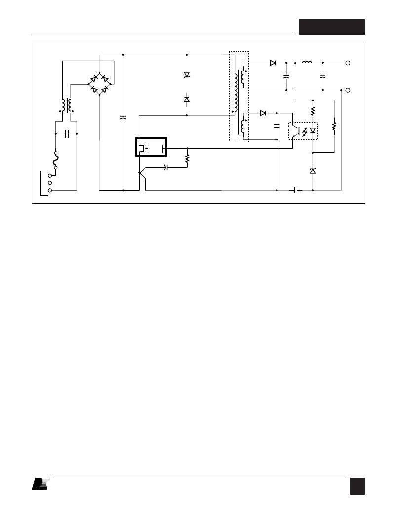
�Figure� 8.� Schematic� Diagram� of� a� 20� W� Universal� Input� TOPSwitch-II� Power� Supply� using� an� 8� lead� PDIP.�
�20� W� Universal� Supply� using� 8� Lead� PDIP�
�Figure� 8� shows� a� 12� V,� 20� W� secondary� regulated� flyback� power�
�supply� using� the� TOP224P� in� an� eight� lead� PDIP� package� and�
�operating� from� universal� 85� to� 265� VAC� input� voltage.� This�
�example� demonstrates� the� advantage� of� the� higher� power� 8� pin�
�leadframe� used� with� the� TOPSwitch-II� family.� This� low� cost�
�package� transfers� heat� directly� to� the� board� through� six� source�
�pins,� eliminating� the� heatsink� and� the� associated� cost.� Efficiency�
�is� typically� 80%� at� low� line� input.� Output� voltage� is� directly�
�sensed� by� optocoupler� U2� and� Zener� diode� VR2.� The� output�
�voltage� is� determined� by� the� Zener� diode� (VR2)� voltage� and� the�
�voltage� drops� across� the� optocoupler� (U2)� LED� and� resistor� R1.�
�Other� output� voltages� are� possible� by� adjusting� the� transformer�
�turns� ratio� and� value� of� Zener� diode� VR2.�
�AC� power� is� rectified� and� filtered� by� BR1� and� C1� to� create� the�
�high� voltage� DC� bus� applied� to� the� primary� winding� of� T1.� The�
�other� side� of� the� transformer� primary� is� driven� by� the� integrated�
�TOPSwitch-II� high-voltage� MOSFET.� D1� and� VR1� clamp�
�leading-edge� voltage� spikes� caused� by� transformer� leakage�
�inductance.� The� power� secondary� winding� is� rectified� and�
�filtered� by� D2,� C2,� L1,� and� C3� to� create� the� 12� V� output� voltage.�
�R2� and� VR2� provide� a� slight� pre-load� on� the� 12� V� output� to�
�improve� load� regulation� at� light� loads.� The� bias� winding� is�
�rectified� and� filtered� by� D3� and� C4� to� create� a� TOPSwitch� bias�
�voltage.� L2� and� Y1-safety� capacitor� C7� attenuate� common�
�mode� emission� currents� caused� by� high� voltage� switching�
�waveforms� on� the� DRAIN� side� of� the� primary� winding� and� the�
�primary� to� secondary� capacitance.� Leakage� inductance� of� L2�
�with� C1� and� C6� attenuates� differential-mode� emission� currents�
�caused� by� the� fundamental� and� harmonics� of� the� trapezoidal� or�
�triangular� primary� current� waveform.� C5� filters� internal�
�MOSFET� gate� drive� charge� current� spikes� on� the� CONTROL�
�pin,� determines� the� auto-restart� frequency,� and� together� with�
�R1� and� R3,� compensates� the� control� loop.�
�D�
�7/01�
�7�
�相关PDF资料 |
PDF描述 |
|---|---|
| VE-21V-CY-F1 | CONVERTER MOD DC/DC 5.8V 50W |
| EBM10DWWH | CONN EDGECARD 20POS .156 SQ WW |
| VI-B1V-CY-F3 | CONVERTER MOD DC/DC 5.8V 50W |
| TOP267KG | IC OFFLINE SWITCHER 45W 65W |
| VI-B1V-CY-F2 | CONVERTER MOD DC/DC 5.8V 50W |
相关代理商/技术参数 |
参数描述 |
|---|---|
| TOP221Y | 功能描述:交流/直流开关转换器 7W 85-265 VAC 12W100/115/230 VAC RoHS:否 制造商:STMicroelectronics 输出电压:800 V 输入/电源电压(最大值):23.5 V 输入/电源电压(最小值):11.5 V 开关频率:115 kHz 电源电流:1.6 mA 工作温度范围:- 40 C to + 150 C 安装风格:SMD/SMT 封装 / 箱体:SSO-10 封装:Reel |
| TOP221YN | 功能描述:交流/直流开关转换器 7W 85-265 VAC 12W100/115/230 VAC RoHS:否 制造商:STMicroelectronics 输出电压:800 V 输入/电源电压(最大值):23.5 V 输入/电源电压(最小值):11.5 V 开关频率:115 kHz 电源电流:1.6 mA 工作温度范围:- 40 C to + 150 C 安装风格:SMD/SMT 封装 / 箱体:SSO-10 封装:Reel |
| TOP222G | 功能描述:交流/直流开关转换器 10W 85-265 VAC 15W100/115/230 VAC RoHS:否 制造商:STMicroelectronics 输出电压:800 V 输入/电源电压(最大值):23.5 V 输入/电源电压(最小值):11.5 V 开关频率:115 kHz 电源电流:1.6 mA 工作温度范围:- 40 C to + 150 C 安装风格:SMD/SMT 封装 / 箱体:SSO-10 封装:Reel |
| TOP222GN | 功能描述:交流/直流开关转换器 10W 85-265 VAC 15W100/115/230 VAC RoHS:否 制造商:STMicroelectronics 输出电压:800 V 输入/电源电压(最大值):23.5 V 输入/电源电压(最小值):11.5 V 开关频率:115 kHz 电源电流:1.6 mA 工作温度范围:- 40 C to + 150 C 安装风格:SMD/SMT 封装 / 箱体:SSO-10 封装:Reel |
| TOP222GN-TL | 功能描述:交流/直流开关转换器 10W 85-265 VAC 15W100/115/230 VAC RoHS:否 制造商:STMicroelectronics 输出电压:800 V 输入/电源电压(最大值):23.5 V 输入/电源电压(最小值):11.5 V 开关频率:115 kHz 电源电流:1.6 mA 工作温度范围:- 40 C to + 150 C 安装风格:SMD/SMT 封装 / 箱体:SSO-10 封装:Reel |
发布紧急采购,3分钟左右您将得到回复。