- 您现在的位置:买卖IC网 > PDF目录19657 > TOP244Y (Power Integrations)IC OFFLINE SWIT UVLO HV TO220 PDF资料下载
参数资料
| 型号: | TOP244Y |
| 厂商: | Power Integrations |
| 文件页数: | 29/52页 |
| 文件大小: | 0K |
| 描述: | IC OFFLINE SWIT UVLO HV TO220 |
| 标准包装: | 2,000 |
| 系列: | TOPSwitch®-GX |
| 输出隔离: | 隔离 |
| 频率范围: | 66 ~ 132kHz |
| 输出电压: | 700V |
| 功率(瓦特): | 65W |
| 工作温度: | -40°C ~ 150°C |
| 封装/外壳: | TO-220-7(成形引线),6 引线 |
| 供应商设备封装: | TO-220-7C |
| 包装: | 管件 |
第1页第2页第3页第4页第5页第6页第7页第8页第9页第10页第11页第12页第13页第14页第15页第16页第17页第18页第19页第20页第21页第22页第23页第24页第25页第26页第27页第28页当前第29页第30页第31页第32页第33页第34页第35页第36页第37页第38页第39页第40页第41页第42页第43页第44页第45页第46页第47页第48页第49页第50页第51页第52页
�� �
�
�TOP242-250�
�Input� Capacitor�
�The� input� capacitor� must� be� chosen� to� provide� the� minimum� DC�
�voltage� required� for� the� TOPSwitch� -� GX� converter� to� maintain�
�regulation� at� the� lowest� speci?ed� input� voltage� and� maximum�
�output� power.� Since� TOPSwitch� -� GX� has� a� higher� DC� MAX� than�
�TOPSwitch-II� ,� it� is� possible� to� use� a� smaller� input� capacitor.�
�For� TOPSwitch� -� GX,� a� capacitance� of� 2� μ� F� per� watt� is� possible� for�
�universal� input� with� an� appropriately� designed� transformer.�
�Primary� Clamp� and� Output� Re?ected� Voltage� V� OR�
�A� primary� clamp� is� necessary� to� limit� the� peak� TOPSwitch� -� GX�
�drain� to� source� voltage.� A� Zener� clamp� requires� few� parts� and�
�takes� up� little� board� space.� For� good� ef?ciency,� the� clamp�
�Zener� should� be� selected� to� be� at� least� 1.5� times� the� output�
�re?ected� voltage� V� OR� ,� as� this� keeps� the� leakage� spike� conduction�
�time� short.� When� using� a� Zener� clamp� in� a� universal� input�
�application,� a� V� OR� of� less� than� 135� V� is� recommended� to� allow�
�for� the� absolute� tolerances� and� temperature� variations� of� the�
�Zener.� This� will� ensure� ef?cient� operation� of� the� clamp� circuit�
�and� will� also� keep� the� maximum� drain� voltage� below� the� rated�
�breakdown� voltage� of� the� TOPSwitch� -� GX� MOSFET.�
�transformer� saturation� during� start-up.� Also,� soft-start� limits� the�
�amount� of� output� voltage� overshoot� and,� in� many� applications,�
�eliminates� the� need� for� a� soft-?nish� capacitor.�
�EMI�
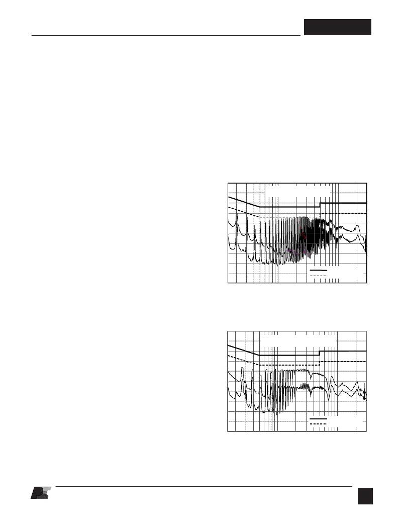
�The� frequency� jitter� feature� modulates� the� switching� frequency�
�over� a� narrow� band� as� a� means� to� reduce� conducted� EMI� peaks�
�associated� with� the� harmonics� of� the� fundamental� switching�
�frequency.� This� is� particularly� bene?cial� for� average� detection�
�mode.� As� can� be� seen� in� Figure� 46,� the� bene?ts� of� jitter� increase�
�with� the� order� of� the� switching� harmonic� due� to� an� increase� in�
�frequency� deviation.�
�The� FREQUENCY� pin� of� TOPSwitch� -� GX� offers� a� switching�
�frequency� option� of� 132� kHz� or� 66� kHz.� In� applications� that�
�require� heavy� snubbers� on� the� drain� node� for� reducing� high�
�80�
�70� TOPSWITCH-II� (NO� JITTER)�
�60�
�50�
�A� high� V� OR� is� required� to� take� full� advantage� of� the� wider� DC� MAX�
�of� TOPSwitch� -� GX.� An� RCD� clamp� provides� tighter� clamp�
�voltage� tolerance� than� a� Zener� clamp� and� allows� a� V� OR� as� high�
�as� 150� V.� RCD� clamp� dissipation� can� be� minimized� by� reducing�
�the� external� current� limit� as� a� function� of� input� line� voltage� (see�
�Figures� 21� and� 35).� The� RCD� clamp� is� more� cost� effective� than�
�the� Zener� clamp� but� requires� more� careful� design� (see� Quick�
�Design� Checklist).�
�40�
�30�
�20�
�-10�
�0�
�-10�
�-20�
�EN55022B� (QP)�
�EN55022B� (AV)�
�-10�
�Output� Diode�
�The� output� diode� is� selected� for� peak� inverse� voltage,� output�
�current,� and� thermal� conditions� in� the� application� (including�
�heatsinking,� air� circulation,� etc.).� The� higher� DC� MAX� of�
�TOPSwitch� -� GX,� along� with� an� appropriate� transformer� turns�
�ratio,� can� allow� the� use� of� a� 60� V� Schottky� diode� for� higher�
�ef?ciency� on� output� voltages� as� high� as� 15� V� (see� Figure� 41:� A�
�12� V,� 30� W� design� using� a� 60� V� Schottky� for� the� output� diode).�
�Bias� Winding� Capacitor�
�Due� to� the� low� frequency� operation� at� no-load� a� 1� μ� F� bias�
�winding� capacitor� is� recommended.�
�Soft-Start�
�Generally,� a� power� supply� experiences� maximum� stress� at�
�start-up� before� the� feedback� loop� achieves� regulation.� For� a�
�period� of� 10� ms,� the� on-chip� soft-start� linearly� increases� the� duty�
�cycle� from� zero� to� the� default� DC� MAX� at� turn� on.� In� addition,�
�the� primary� current� limit� increases� from� 85%� to� 100%� over� the�
�same� period.� This� causes� the� output� voltage� to� rise� in� an� orderly�
�manner,� allowing� time� for� the� feedback� loop� to� take� control� of�
�the� duty� cycle.� This� reduces� the� stress� on� the� TOPSwitch-GX�
�MOSFET,� clamp� circuit� and� output� diode(s),� and� helps� prevent�
�0.15� 1� 10� 30�
�FREQUENCY� (MHZ)�
�Figure� 46a.� TOPSwitch-II� Full� Range� EMI� Scan� (100� kHz,� No� Jitter).�
�80�
�70� TOPSWITCH-GX� (WITH JITTER)�
�60�
�50�
�40�
�30�
�20�
�-10�
�0�
�EN55022B� (QP)�
�EN55022B� (AV)�
�-20�
�0.15� 1� 10� 30�
�FREQUENCY� (MHZ)�
�Figure� 46b.� TOPSwitch-GX� Full� Range� EMI� Scan� (132� kHz,� With�
�Jitter)� with� Identical� Circuitry� and� Conditions.�
�O�
�11/05�
�29�
�相关PDF资料 |
PDF描述 |
|---|---|
| VE-BWP-CW-B1 | CONVERTER MOD DC/DC 13.8V 100W |
| RSM44DSXS | CONN EDGECARD 88POS DIP .156 SLD |
| VE-BWN-CW-B1 | CONVERTER MOD DC/DC 18.5V 100W |
| NCP1219AD65R2G | IC CTRLR PWM CM OVP OTP HV 7SOIC |
| GBC20DRXI | CONN EDGECARD 40POS DIP .100 SLD |
相关代理商/技术参数 |
参数描述 |
|---|---|
| TOP244Y- | 制造商:POWERINT 制造商全称:Power Integrations, Inc. 功能描述:TOPSwitch-GX Family Extended Power, Design Flexible, EcoSmart, Integrated Off-line Switcher |
| TOP244Y/F | 制造商:未知厂家 制造商全称:未知厂家 功能描述:Up to 290 W Extended power. design flexible. |
| TOP244YN | 功能描述:交流/直流开关转换器 45 W 85-265 VAC 65 W 230 VAC RoHS:否 制造商:STMicroelectronics 输出电压:800 V 输入/电源电压(最大值):23.5 V 输入/电源电压(最小值):11.5 V 开关频率:115 kHz 电源电流:1.6 mA 工作温度范围:- 40 C to + 150 C 安装风格:SMD/SMT 封装 / 箱体:SSO-10 封装:Reel |
| TOP244YN- | 制造商:POWERINT 制造商全称:Power Integrations, Inc. 功能描述:TOPSwitch-GX Family Extended Power, Design Flexible, EcoSmart, Integrated Off-line Switcher |
| TOP244YN-TL | 制造商:POWERINT 制造商全称:Power Integrations, Inc. 功能描述:TOPSwitch-GX Family Extended Power, Design Flexible, EcoSmart, Integrated Off-line Switcher |
发布紧急采购,3分钟左右您将得到回复。