- 您现在的位置:买卖IC网 > PDF目录19717 > TOP245PN (Power Integrations)IC OFFLINE SWIT OVP UVLO HV 8DIP PDF资料下载
参数资料
| 型号: | TOP245PN |
| 厂商: | Power Integrations |
| 文件页数: | 5/52页 |
| 文件大小: | 0K |
| 描述: | IC OFFLINE SWIT OVP UVLO HV 8DIP |
| 标准包装: | 50 |
| 输出隔离: | 隔离 |
| 频率范围: | 66 ~ 132kHz |
| 输出电压: | 700V |
| 功率(瓦特): | 30W |
| 工作温度: | -40°C ~ 150°C |
| 封装/外壳: | 8-DIP(0.300",7.62mm),7 引线 |
| 供应商设备封装: | DIP-8B |
| 包装: | 管件 |
| 产品目录页面: | 1204 (CN2011-ZH PDF) |
| 其它名称: | 596-1074-5 |
第1页第2页第3页第4页当前第5页第6页第7页第8页第9页第10页第11页第12页第13页第14页第15页第16页第17页第18页第19页第20页第21页第22页第23页第24页第25页第26页第27页第28页第29页第30页第31页第32页第33页第34页第35页第36页第37页第38页第39页第40页第41页第42页第43页第44页第45页第46页第47页第48页第49页第50页第51页第52页
�� �
�
�TOP242-250�
�TOPSwitch-GX� Family� Functional�
�Description�
�Like� TOPSwitch� ,� TOPSwitch-GX� is� an� integrated� switched�
�mode� power� supply� chip� that� converts� a� current� at� the� control�
�input� to� a� duty� cycle� at� the� open� drain� output� of� a� high� voltage�
�power� MOSFET.� During� normal� operation� the� duty� cycle�
�of� the� power� MOSFET� decreases� linearly� with� increasing�
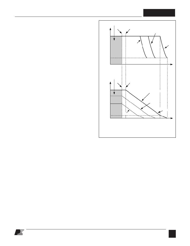
�CONTROL� pin� current� as� shown� in� Figure� 7.�
�AUTO-RESTART�
�I� CD1�
�132�
�I� B�
�I� L� =� 190� μ� A�
�I� L� =� 125� μ� A�
�I� L� <� I� L(DC)�
�In� addition� to� the� three� terminal� TOPSwitch� features,� such� as�
�the� high� voltage� start-up,� the� cycle-by-cycle� current� limiting,�
�loop� compensation� circuitry,� auto-restart,� thermal� shutdown,�
�the� TOPSwitch-GX� incorporates� many� additional� functions� that�
�reduce� system� cost,� increase� power� supply� performance� and�
�design� ?exibility.� A� patented� high� voltage� CMOS� technology�
�allows� both� the� high� voltage� power� MOSFET� and� all� the� low�
�voltage� control� circuitry� to� be� cost� effectively� integrated� onto�
�a� single� monolithic� chip.�
�30�
�AUTO-RESTART�
�I� CD1�
�78�
�I� B�
�I� C� (MA)�
�SLOPE� =� PWM� GAIN�
�I� L� =� 190� μ� A�
�Three� terminals,� FREQUENCY,� LINE-SENSE,� and�
�EXTERNAL� CURRENT� LIMIT� (available� in� Y,� R� or� F�
�package)� or� one� terminal� MULTI-FUNCTION� (available� in� P�
�or� G� package)� have� been� added� to� implement� some� of� the� new�
�functions.� These� terminals� can� be� connected� to� the� SOURCE�
�pin� to� operate� the� TOPSwitch-GX� in� a� TOPSwitch� -like� three�
�terminal� mode.� However,� even� in� this� three� terminal� mode,� the�
�TOPSwitch-GX� offers� many� new� transparent� features� that� do�
�not� require� any� external� components:�
�38�
�10�
�TOP242-5� 1.6� 2.0�
�TOP246-9� 2.2� 2.6�
�TOP250� 2.4� 2.7�
�I� C� (MA)�
�I� L� =� 125� μ� A�
�I� L� <� I� L(DC)�
�5.2� 6.0�
�5.8� 6.6�
�6.5� 7.3�
�1.� A� fully� integrated� 10� ms� soft-start� limits� peak� currents�
�and� voltages� during� start-up� and� dramatically� reduces� or�
�eliminates� output� overshoot� in� most� applications.�
�2.� DC� MAX� of� 78%� allows� smaller� input� storage� capacitor,� lower�
�input� voltage� requirement� and/or� higher� power� capability.�
�3.� Frequency� reduction� at� light� loads� lowers� the� switching�
�losses� and� maintains� good� cross� regulation� in� multiple� output�
�supplies.�
�4.� Higher� switching� frequency� of� 132� kHz� reduces� the�
�transformer� size� with� no� noticeable� impact� on� EMI.�
�5.� Frequency� jittering� reduces� EMI.�
�6.� Hysteretic� over-temperature� shutdown� ensures� automatic�
�recovery� from� thermal� fault.� Large� hysteresis� prevents�
�circuit� board� overheating.�
�7.� Packages� with� omitted� pins� and� lead� forming� provide� large�
�drain� creepage� distance.�
�8.� Tighter� absolute� tolerances� and� smaller� temperature�
�variations� on� switching� frequency,� current� limit� and� PWM� gain.�
�The� LINE-SENSE� (L)� pin� is� usually� used� for� line� sensing� by�
�connecting� a� resistor� from� this� pin� to� the� recti?ed� DC� high�
�voltage� bus� to� implement� line� overvoltage� (OV),� under-voltage�
�(UV)� and� line� feed-forward� with� DC� MAX� reduction.� In� this�
�mode,� the� value� of� the� resistor� determines� the� OV/UV� thresholds�
�and� the� DC� MAX� is� reduced� linearly� starting� from� a� line� voltage�
�above� the� under-voltage� threshold.� See� Table� 2� and� Figure� 11.�
�NOTE:� FOR� P� AND� G� PACKAGES� I� L� IS� REPLACED� WITH� I� M� .�
�PI-2633-011502�
�Figure� 7.� Relationship� of� Duty� Cycle� and� Frequency� to� CONTROL�
�Pin� Current.�
�The� pin� can� also� be� used� as� a� remote� ON/OFF� and� a�
�synchronization� input.�
�The� EXTERNAL� CURRENT� LIMIT� (X)� pin� is� usually� used�
�to� reduce� the� current� limit� externally� to� a� value� close� to� the�
�operating� peak� current,� by� connecting� the� pin� to� SOURCE�
�through� a� resistor.� This� pin� can� also� be� used� as� a� remote�
�ON/OFF� and� a� synchronization� input� in� both� modes.� See�
�Table� 2� and� Figure� 11.�
�For� the� P� or� G� packages� the� LINE-SENSE� and� EXTERNAL�
�CURRENT� LIMIT� pin� functions� are� combined� on� one� MULTI-�
�FUNCTION� (M)� pin.� However,� some� of� the� functions� become�
�mutually� exclusive� as� shown� in� Table� 3.�
�The� FREQUENCY� (F)� pin� in� the� Y,� R� or� F� package� sets� the�
�switching� frequency� to� the� default� value� of� 132� kHz� when�
�connected� to� SOURCE� pin.� A� half� frequency� option� of�
�66� kHz� can� be� chosen� by� connecting� this� pin� to� CONTROL� pin�
�instead.� Leaving� this� pin� open� is� not� recommended.�
�O�
�11/05�
�5�
�相关PDF资料 |
PDF描述 |
|---|---|
| ACM28DSAN | CONN EDGECARD 56POS R/A .156 SLD |
| 172-E15-202R031 | CONN DB15 FEMALE SLD CUP TIN |
| ACM28DSAH | CONN EDGECARD 56POS R/A .156 SLD |
| EEM28DRUS | CONN EDGECARD 56POS DIP .156 SLD |
| ECM12DRUI | CONN EDGECARD 24POS DIP .156 SLD |
相关代理商/技术参数 |
参数描述 |
|---|---|
| TOP245PN- | 制造商:POWERINT 制造商全称:Power Integrations, Inc. 功能描述:TOPSwitch-GX Family Extended Power, Design Flexible, EcoSmart, Integrated Off-line Switcher |
| TOP245PN0152 | 制造商:Power Integrations 功能描述: |
| TOP245PN-TL | 制造商:POWERINT 制造商全称:Power Integrations, Inc. 功能描述:TOPSwitch-GX Family Extended Power, Design Flexible, EcoSmart, Integrated Off-line Switcher |
| TOP245P-TL | 制造商:POWERINT 制造商全称:Power Integrations, Inc. 功能描述:TOPSwitch-GX Family Extended Power, Design Flexible, EcoSmart, Integrated Off-line Switcher |
| TOP245R | 制造商:POWERINT 制造商全称:Power Integrations, Inc. 功能描述:Family Extended Power, Design Flexible,Integrated Off-line Switcher |
发布紧急采购,3分钟左右您将得到回复。