- 您现在的位置:买卖IC网 > PDF目录22107 > TOP246FN (Power Integrations)IC OFFLINE SWIT UVLO HV TO262 PDF资料下载
参数资料
| 型号: | TOP246FN |
| 厂商: | Power Integrations |
| 文件页数: | 6/52页 |
| 文件大小: | 0K |
| 描述: | IC OFFLINE SWIT UVLO HV TO262 |
| 标准包装: | 50 |
| 系列: | TOPSwitch®-GX |
| 输出隔离: | 隔离 |
| 频率范围: | 66 ~ 132kHz |
| 输出电压: | 700V |
| 功率(瓦特): | 125W |
| 工作温度: | -40°C ~ 150°C |
| 封装/外壳: | TO-262-7(成形引线),6 引线 |
| 供应商设备封装: | TO-262-7C |
| 包装: | 管件 |
| 产品目录页面: | 1204 (CN2011-ZH PDF) |
| 其它名称: | 596-1168 TOP246FN-ND |
第1页第2页第3页第4页第5页当前第6页第7页第8页第9页第10页第11页第12页第13页第14页第15页第16页第17页第18页第19页第20页第21页第22页第23页第24页第25页第26页第27页第28页第29页第30页第31页第32页第33页第34页第35页第36页第37页第38页第39页第40页第41页第42页第43页第44页第45页第46页第47页第48页第49页第50页第51页第52页
�� �
�
�TOP242-250�
�CONTROL� (C)� Pin� Operation�
�The� CONTROL� pin� is� a� low� impedance� node� that� is� capable�
�of� receiving� a� combined� supply� and� feedback� current.� During�
�normal� operation,� a� shunt� regulator� is� used� to� separate� the�
�feedback� signal� from� the� supply� current.� CONTROL� pin� voltage�
�V� C� is� the� supply� voltage� for� the� control� circuitry� including� the�
�MOSFET� gate� driver.� An� external� bypass� capacitor� closely�
�connected� between� the� CONTROL� and� SOURCE� pins� is� required�
�to� supply� the� instantaneous� gate� drive� current.� The� total� amount�
�of� capacitance� connected� to� this� pin� also� sets� the� auto-restart�
�timing� as� well� as� control� loop� compensation.�
�When� recti?ed� DC� high� voltage� is� applied� to� the� DRAIN�
�pin� during� start-up,� the� MOSFET� is� initially� off,� and� the�
�CONTROL� pin� capacitor� is� charged� through� a� switched� high�
�voltage� current� source� connected� internally� between� the� DRAIN�
�and� CONTROL� pins.� When� the� CONTROL� pin� voltage� V� C�
�reaches� approximately� 5.8� V,� the� control� circuitry� is� activated�
�and� the� soft-start� begins.� The� soft-start� circuit� gradually�
�increases� the� duty� cycle� of� the� MOSFET� from� zero� to� the�
�maximum� value� over� approximately� 10� ms.� If� no� external�
�feedback/supply� current� is� fed� into� the� CONTROL� pin� by� the�
�end� of� the� soft-start,� the� high� voltage� current� source� is� turned�
�off� and� the� CONTROL� pin� will� start� discharging� in� response�
�to� the� supply� current� drawn� by� the� control� circuitry.� If� the�
�power� supply� is� designed� properly,� and� no� fault� condition�
�such� as� open� loop� or� shorted� output� exists,� the� feedback� loop�
�will� close,� providing� external� CONTROL� pin� current,� before�
�the� CONTROL� pin� voltage� has� had� a� chance� to� discharge� to�
�the� lower� threshold� voltage� of� approximately� 4.8� V� (internal�
�supply� under-voltage� lockout� threshold).� When� the� externally�
�fed� current� charges� the� CONTROL� pin� to� the� shunt� regulator�
�V� UV�
�V� LINE�
�0� V�
�voltage� of� 5.8� V,� current� in� excess� of� the� consumption� of� the�
�chip� is� shunted� to� SOURCE� through� resistor� R� E� as� shown� in�
�Figure� 2.� This� current� ?owing� through� R� E� controls� the� duty� cycle�
�of� the� power� MOSFET� to� provide� closed� loop� regulation.� The�
�shunt� regulator� has� a� ?nite� low� output� impedance� Z� C� that� sets�
�the� gain� of� the� error� ampli?er� when� used� in� a� primary� feedback�
�con?guration.� The� dynamic� impedance� Z� C� of� the� CONTROL�
�pin� together� with� the� external� CONTROL� pin� capacitance� sets�
�the� dominant� pole� for� the� control� loop.�
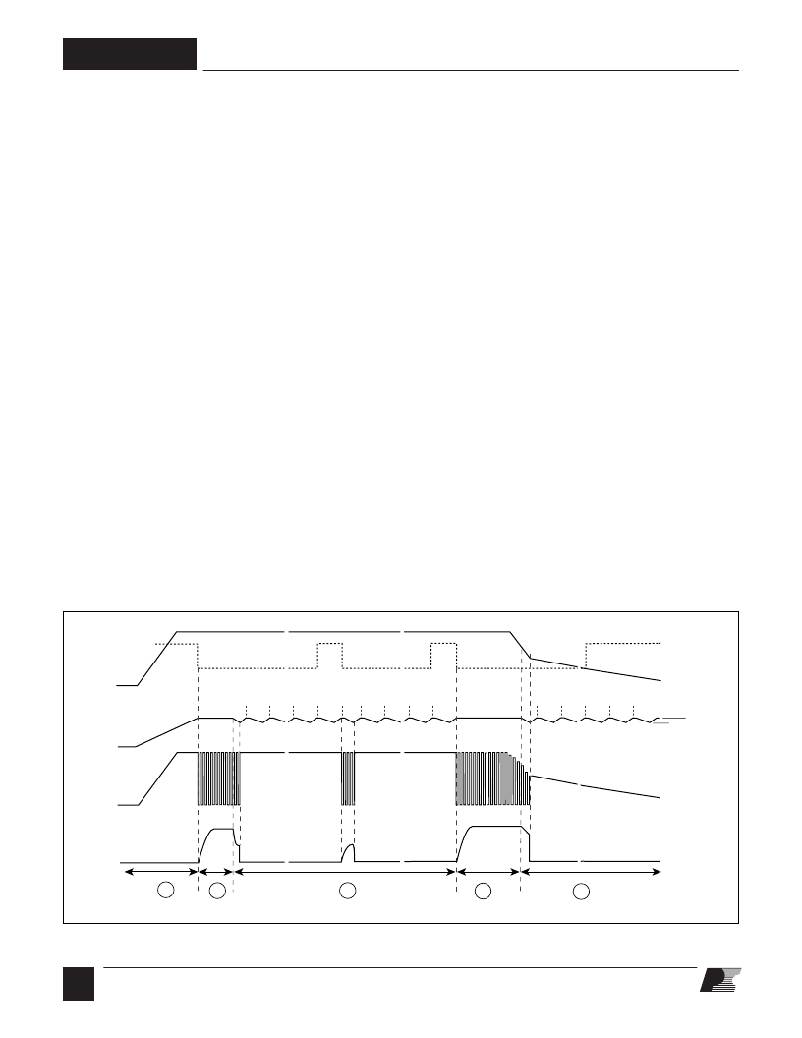
�When� a� fault� condition� such� as� an� open� loop� or� shorted� output�
�prevents� the� ?ow� of� an� external� current� into� the� CONTROL�
�pin,� the� capacitor� on� the� CONTROL� pin� discharges� towards�
�4.8� V.� At� 4.8� V,� auto-restart� is� activated� which� turns� the� output�
�MOSFET� off� and� puts� the� control� circuitry� in� a� low� current�
�standby� mode.� The� high-voltage� current� source� turns� on� and�
�charges� the� external� capacitance� again.� A� hysteretic� internal�
�supply� under-voltage� comparator� keeps� V� C� within� a� window�
�of� typically� 4.8� V� to� 5.8� V� by� turning� the� high-voltage� current�
�source� on� and� off� as� shown� in� Figure� 8.� The� auto-restart�
�circuit� has� a� divide-by-eight� counter� which� prevents� the� output�
�MOSFET� from� turning� on� again� until� eight� discharge/charge�
�cycles� have� elapsed.� This� is� accomplished� by� enabling� the�
�output� MOSFET� only� when� the� divide-by-eight� counter� reaches�
�full� count� (S7).� The� counter� effectively� limits� TOPSwitch-GX�
�power� dissipation� by� reducing� the� auto-restart� duty� cycle�
�to� typically� 4%.� Auto-restart� mode� continues� until� output�
�voltage� regulation� is� again� achieved� through� closure� of� the�
�feedback� loop.�
�Oscillator� and� Switching� Frequency�
�The� internal� oscillator� linearly� charges� and� discharges� an�
�V� C�
�S7�
�S0�
�S1�
�S2�
�S6�
�S7�
�S0�
�S1�
�S2�
�S6�
�S7�
�S0�
�S1�
�S2�
�S6�
�S7�
�S7�
�5.8� V�
�4.8� V�
�0� V�
�V� DRAIN�
�0� V�
�V� OUT�
�0� V�
�1�
�2�
�3�
�2�
�4�
�NOTE:� S0� THROUGH� S7� ARE� THE� OUTPUT� STATES� OF� THE� AUTO-RESTART� COUNTER�
�Figure� 8.� Typical� Waveforms� for� (1)� Power� Up� (2)� Normal� Operation� (3)� Auto-Restart� (4)� Power� Down.�
�PI-2545-082299�
�6�
�O�
�11/05�
�相关PDF资料 |
PDF描述 |
|---|---|
| ADM1275-1ACPZ | IC HOT SWAP CTRL PMBUS 20LFCSP |
| VI-23B-EV-F2 | CONVERTER MOD DC/DC 95V 150W |
| RSM44DRUS | CONN EDGECARD 88POS DIP .156 SLD |
| 1-530844-7 | CONN CARDEDGE II 28POS PCB GOLD |
| VI-23B-EV-F1 | CONVERTER MOD DC/DC 95V 150W |
相关代理商/技术参数 |
参数描述 |
|---|---|
| TOP246FN- | 制造商:POWERINT 制造商全称:Power Integrations, Inc. 功能描述:TOPSwitch-GX Family Extended Power, Design Flexible, EcoSmart, Integrated Off-line Switcher |
| TOP246FN-TL | 制造商:POWERINT 制造商全称:Power Integrations, Inc. 功能描述:TOPSwitch-GX Family Extended Power, Design Flexible, EcoSmart, Integrated Off-line Switcher |
| TOP246F-TL | 制造商:POWERINT 制造商全称:Power Integrations, Inc. 功能描述:TOPSwitch-GX Family Extended Power, Design Flexible, EcoSmart, Integrated Off-line Switcher |
| TOP246G- | 制造商:POWERINT 制造商全称:Power Integrations, Inc. 功能描述:TOPSwitch-GX Family Extended Power, Design Flexible, EcoSmart, Integrated Off-line Switcher |
| TOP246GN | 功能描述:交流/直流开关转换器 22W 85-265 VAC 30 W 230 VAC RoHS:否 制造商:STMicroelectronics 输出电压:800 V 输入/电源电压(最大值):23.5 V 输入/电源电压(最小值):11.5 V 开关频率:115 kHz 电源电流:1.6 mA 工作温度范围:- 40 C to + 150 C 安装风格:SMD/SMT 封装 / 箱体:SSO-10 封装:Reel |
发布紧急采购,3分钟左右您将得到回复。