- 您现在的位置:买卖IC网 > PDF目录19722 > TOP257EG (Power Integrations)IC OFFLINE SWIT PROG OVP 7CESIP PDF资料下载
参数资料
| 型号: | TOP257EG |
| 厂商: | Power Integrations |
| 文件页数: | 9/50页 |
| 文件大小: | 0K |
| 描述: | IC OFFLINE SWIT PROG OVP 7CESIP |
| 标准包装: | 48 |
| 输出隔离: | 隔离 |
| 频率范围: | 66 ~ 132kHz |
| 输出电压: | 700V |
| 功率(瓦特): | 157W |
| 工作温度: | -40°C ~ 150°C |
| 封装/外壳: | 7-SIP,6 引线,裸露焊盘,成形引线 |
| 供应商设备封装: | eSIP-7C |
| 包装: | 管件 |
| 其它名称: | 596-1333-5 |
第1页第2页第3页第4页第5页第6页第7页第8页当前第9页第10页第11页第12页第13页第14页第15页第16页第17页第18页第19页第20页第21页第22页第23页第24页第25页第26页第27页第28页第29页第30页第31页第32页第33页第34页第35页第36页第37页第38页第39页第40页第41页第42页第43页第44页第45页第46页第47页第48页第49页第50页
�� �
�
�TOP252-262�
�Switching�
�Frequency�
�V� DRAIN�
�f� OSC� +�
�f� OSC� -�
�4� ms�
�Time�
�packages).� Duty� cycle� is� reduced� from� DC� MAX� through� the�
�reduction� of� the� on-time� when� I� C� is� increased� beyond� I� B� .� This�
�operation� is� identical� to� the� PWM� control� of� all� other� TOPSwitch�
�families.� TOPSwitch-HX� only� operates� in� this� mode� if� the�
�cycle-by-cycle� peak� drain� current� stays� above� k� PS(UPPER)� *I� LIMIT� (set),�
�where� k� PS(UPPER)� is� 55%� (typical)� and� I� LIMIT� (set)� is� the� current� limit�
�externally� set� via� the� X� or� M� pin.�
�Variable� Frequency� PWM� mode:� When� peak� drain� current� is�
�lowered� to� k� PS(UPPER)� *� I� LIMIT� (set)� as� a� result� of� power� supply� load�
�reduction,� the� PWM� modulator� initiates� the� transition� to� variable�
�frequency� PWM� mode,� and� gradually� turns� off� frequency� jitter.�
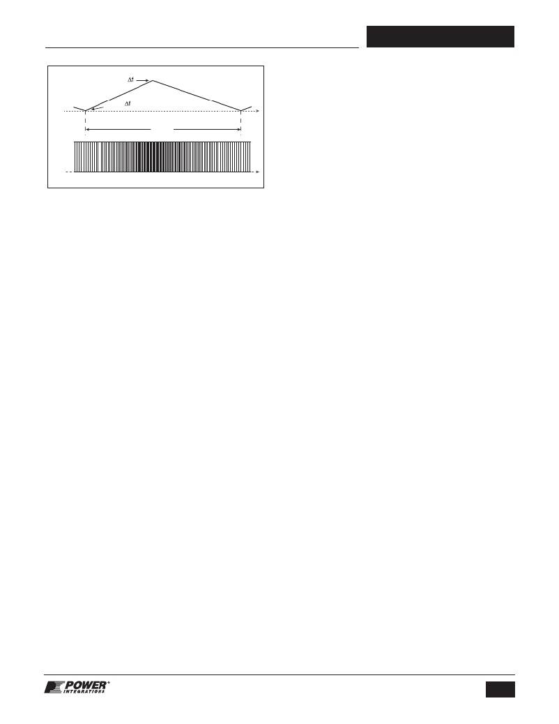
�Figure� 10.� Switching� Frequency� Jitter� (Idealized� V� DRAIN� Waveforms).�
�(half� frequency),� which� may� be� preferable� in� some� cases� such�
�as� noise� sensitive� video� applications� or� a� high� efficiency�
�standby� mode.� Otherwise,� the� FREQUENCY� pin� should� be�
�connected� to� the� SOURCE� pin� for� the� default� 132� kHz.� In� the�
�M,� P� and� G� packages� and� the� TOP259-261� Y� package� option,�
�the� full� frequency� PWM� mode� is� set� at� 66� kHz,� for� higher�
�efficiency� and� increased� output� power� in� all� applications.�
�To� further� reduce� the� EMI� level,� the� switching� frequency� in� the�
�full� frequency� PWM� mode� is� jittered� (frequency� modulated)� by�
�approximately� ±2.5� kHz� for� 66� kHz� operation� or� ±5� kHz� for�
�132� kHz� operation� at� a� 250� Hz� (typical)� rate� as� shown� in�
�Figure� 10.� The� jitter� is� turned� off� gradually� as� the� system� is�
�entering� the� variable� frequency� mode� with� a� fixed� peak� drain�
�current.�
�Pulse� Width� Modulator�
�The� pulse� width� modulator� implements� multi-mode� control� by�
�driving� the� output� MOSFET� with� a� duty� cycle� inversely�
�proportional� to� the� current� into� the� CONTROL� pin� that� is� in�
�excess� of� the� internal� supply� current� of� the� chip� (see� Figure� 9).�
�The� feedback� error� signal,� in� the� form� of� the� excess� current,� is�
�filtered� by� an� RC� network� with� a� typical� corner� frequency� of�
�7� kHz� to� reduce� the� effect� of� switching� noise� in� the� chip� supply�
�current� generated� by� the� MOSFET� gate� driver.�
�To� optimize� power� supply� efficiency,� four� different� control�
�modes� are� implemented.� At� maximum� load,� the� modulator�
�operates� in� full� frequency� PWM� mode;� as� load� decreases,� the�
�modulator� automatically� transitions,� first� to� variable� frequency�
�PWM� mode,� then� to� low� frequency� PWM� mode.� At� light� load,�
�the� control� operation� switches� from� PWM� control� to� multi-cycle-�
�modulation� control,� and� the� modulator� operates� in� multi-cycle-�
�modulation� mode.� Although� different� modes� operate� differently�
�to� make� transitions� between� modes� smooth,� the� simple�
�relationship� between� duty� cycle� and� excess� CONTROL� pin�
�current� shown� in� Figure� 9� is� maintained� through� all� three� PWM�
�modes.� Please� see� the� following� sections� for� the� details� of� the�
�operation� of� each� mode� and� the� transitions� between� modes.�
�Full� Frequency� PWM� mode:� The� PWM� modulator� enters� full�
�frequency� PWM� mode� when� the� CONTROL� pin� current� (I� C� )�
�reaches� I� B� .� In� this� mode,� the� average� switching� frequency� is�
�kept� constant� at� f� OSC� (66� kHz� for� P,� G� and� M� packages� and�
�TOP259-261� Y,� pin� selectable� 132� kHz� or� 66� kHz� for� Y� and� E/L�
�www.powerint.com�
�In� this� mode,� peak� drain� current� is� held� constant� at� k� PS(UPPER)� *�
�I� LIMIT� (set)� while� switching� frequency� drops� from� the� initial� full�
�frequency� of� f� OSC� (132� kHz� or� 66� kHz)� towards� the� minimum�
�frequency� of� f� MCM(MIN)� (30� kHz� typical).� Duty� cycle� reduction� is�
�accomplished� by� extending� the� off-time.�
�Low� Frequency� PWM� mode:� When� switching� frequency�
�reaches� f� MCM(MIN)� (30� kHz� typical),� the� PWM� modulator� starts� to�
�transition� to� low� frequency� mode.� In� this� mode,� switching�
�frequency� is� held� constant� at� f� MCM(MIN)� and� duty� cycle� is� reduced,�
�similar� to� the� full� frequency� PWM� mode,� through� the� reduction�
�of� the� on-time.� Peak� drain� current� decreases� from� the� initial�
�value� of� k� PS(UPPER)� *� I� LIMIT� (set)� towards� the� minimum� value� of�
�k� PS(LOWER)� *I� LIMIT� (set),� where� k� PS(LOWER)� is� 25%� (typical)� and� I� LIMIT� (set)� is�
�the� current� limit� externally� set� via� the� X� or� M� pin.�
�Multi-Cycle-Modulation� mode:� When� peak� drain� current� is�
�lowered� to� k� PS(LOWER)� *I� LIMIT� (set),� the� modulator� transitions� to�
�multi-cycle-modulation� mode.� In� this� mode,� at� each� turn-on,�
�the� modulator� enables� output� switching� for� a� period� of� T� MCM(MIN)�
�at� the� switching� frequency� of� f� MCM(MIN)� (4� or� 5� consecutive� pulses�
�at� 30� kHz)� with� the� peak� drain� current� of� k� PS(LOWER)� *I� LIMIT� (set),� and�
�stays� off� until� the� CONTROL� pin� current� falls� below� I� C(OFF)� .� This�
�mode� of� operation� not� only� keeps� peak� drain� current� low� but�
�also� minimizes� harmonic� frequencies� between� 6� kHz� and�
�30� kHz.� By� avoiding� transformer� resonant� frequency� this� way,�
�all� potential� transformer� audible� noises� are� greatly� suppressed.�
�Maximum� Duty� Cycle�
�The� maximum� duty� cycle,� DC� MAX� ,� is� set� at� a� default� maximum�
�value� of� 78%� (typical).� However,� by� connecting� the� VOLTAGE-�
�MONITOR� or� MULTI-FUNCTION� pin� (depending� on� the�
�package)� to� the� rectified� DC� high� voltage� bus� through� a� resistor�
�with� appropriate� value� (4� M� W� typical),� the� maximum� duty� cycle�
�can� be� made� to� decrease� from� 78%� to� 40%� (typical)� when� input�
�line� voltage� increases� from� 88� V� to� 380� V,� with� dual� gain� slopes.�
�Error� Amplifier�
�The� shunt� regulator� can� also� perform� the� function� of� an� error�
�amplifier� in� primary� side� feedback� applications.� The� shunt�
�regulator� voltage� is� accurately� derived� from� a� temperature-�
�compensated� bandgap� reference.� The� CONTROL� pin� dynamic�
�impedance� Z� C� sets� the� gain� of� the� error� amplifier.� The�
�CONTROL� pin� clamps� external� circuit� signals� to� the� V� C� voltage�
�level.� The� CONTROL� pin� current� in� excess� of� the� supply� current�
�is� separated� by� the� shunt� regulator� and� becomes� the� feedback�
�current� I� fb� for� the� pulse� width� modulator.�
�9�
�Rev.� H� 06/13�
�相关PDF资料 |
PDF描述 |
|---|---|
| ISPLSI 5256VE-80LF256I | IC PLD ISP 144I/O 12NS 256FPBGA |
| GSM44DRTH-S13 | CONN EDGECARD 88POS .156 EXTEND |
| GMM44DRTH-S13 | CONN EDGECARD 88POS .156 EXTEND |
| ABM28DTBT | CONN EDGECARD 56POS R/A .156 SLD |
| 171-025-113R001 | CONN DB25 MALE DIP SOLDER NICKEL |
相关代理商/技术参数 |
参数描述 |
|---|---|
| TOP257EN | 功能描述:交流/直流开关转换器 Int Off-Line Switchr 119W/157W RoHS:否 制造商:STMicroelectronics 输出电压:800 V 输入/电源电压(最大值):23.5 V 输入/电源电压(最小值):11.5 V 开关频率:115 kHz 电源电流:1.6 mA 工作温度范围:- 40 C to + 150 C 安装风格:SMD/SMT 封装 / 箱体:SSO-10 封装:Reel |
| TOP257GN | 功能描述:交流/直流开关转换器 30W/45W PK 85-264VAC 41W/70W PK (230V AC) RoHS:否 制造商:STMicroelectronics 输出电压:800 V 输入/电源电压(最大值):23.5 V 输入/电源电压(最小值):11.5 V 开关频率:115 kHz 电源电流:1.6 mA 工作温度范围:- 40 C to + 150 C 安装风格:SMD/SMT 封装 / 箱体:SSO-10 封装:Reel |
| TOP257GN-TL | 功能描述:交流/直流开关转换器 Off-Line Switcher IC 30W/45W PK RoHS:否 制造商:STMicroelectronics 输出电压:800 V 输入/电源电压(最大值):23.5 V 输入/电源电压(最小值):11.5 V 开关频率:115 kHz 电源电流:1.6 mA 工作温度范围:- 40 C to + 150 C 安装风格:SMD/SMT 封装 / 箱体:SSO-10 封装:Reel |
| TOP257LG | 功能描述:交流/直流开关转换器 78W (85-264VAC) 105W (230V AC) RoHS:否 制造商:STMicroelectronics 输出电压:800 V 输入/电源电压(最大值):23.5 V 输入/电源电压(最小值):11.5 V 开关频率:115 kHz 电源电流:1.6 mA 工作温度范围:- 40 C to + 150 C 安装风格:SMD/SMT 封装 / 箱体:SSO-10 封装:Reel |
| TOP257LN | 功能描述:交流/直流开关转换器 78W (85-264VAC) 105W (230V AC) RoHS:否 制造商:STMicroelectronics 输出电压:800 V 输入/电源电压(最大值):23.5 V 输入/电源电压(最小值):11.5 V 开关频率:115 kHz 电源电流:1.6 mA 工作温度范围:- 40 C to + 150 C 安装风格:SMD/SMT 封装 / 箱体:SSO-10 封装:Reel |
发布紧急采购,3分钟左右您将得到回复。