- 您现在的位置:买卖IC网 > PDF目录19883 > TOP260EG (Power Integrations)IC OFFLINE SWIT PROG OVP 7CESIP PDF资料下载
参数资料
| 型号: | TOP260EG |
| 厂商: | Power Integrations |
| 文件页数: | 10/50页 |
| 文件大小: | 0K |
| 描述: | IC OFFLINE SWIT PROG OVP 7CESIP |
| 标准包装: | 48 |
| 输出隔离: | 隔离 |
| 频率范围: | 66 ~ 132kHz |
| 输出电压: | 700V |
| 功率(瓦特): | 275W |
| 工作温度: | -40°C ~ 150°C |
| 封装/外壳: | 7-SIP,6 引线,裸露焊盘,成形引线 |
| 供应商设备封装: | eSIP-7C |
| 包装: | 管件 |
| 其它名称: | 596-1338-5 |
第1页第2页第3页第4页第5页第6页第7页第8页第9页当前第10页第11页第12页第13页第14页第15页第16页第17页第18页第19页第20页第21页第22页第23页第24页第25页第26页第27页第28页第29页第30页第31页第32页第33页第34页第35页第36页第37页第38页第39页第40页第41页第42页第43页第44页第45页第46页第47页第48页第49页第50页
�� �
�
�TOP252-262�
�V� UV�
�V� LINE�
�0V�
�V� C�
�S15�
�S14�
�S13� S12�
�S0�
�S15� S14�
�S13�
�S12�
�S0�
�S15�
�S14�
�S13�
�S12�
�S0�
�S15�
�S15�
�5.8� V�
�4.8� V�
�0V�
�V� DRAIN�
�0V�
�V� OUT�
�0V�
�1�
�2�
�3�
�2�
�4�
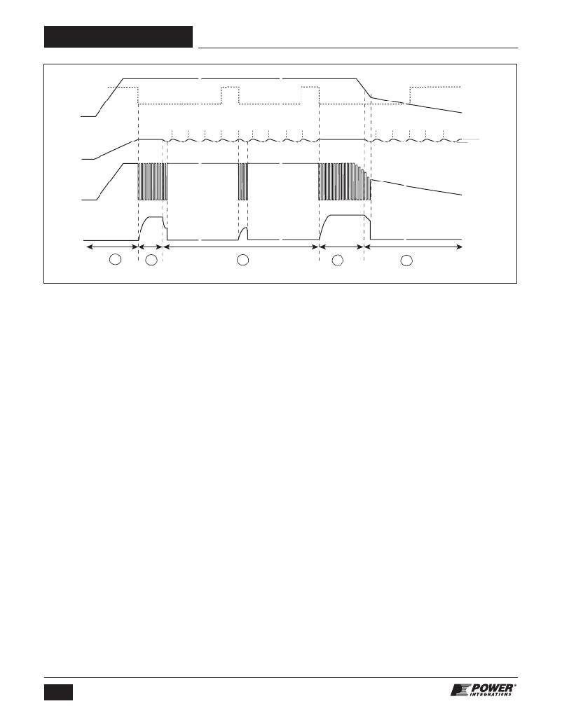
�Note:� S0� through� S15� are� the� output� states� of� the� auto-restart� counter�
�Figure� 11.� Typical� Waveforms� for� (1)� Power� Up� (2)� Normal� Operation� (3)� Auto-Restart� (4)� Power� Down.�
�PI-4531-121206�
�On-Chip� Current� Limit� with� External� Programmability�
�The� cycle-by-cycle� peak� drain� current� limit� circuit� uses� the�
�output� MOSFET� ON-resistance� as� a� sense� resistor.� A� current�
�limit� comparator� compares� the� output� MOSFET� on-state� drain�
�to� source� voltage� V� DS(ON)� with� a� threshold� voltage.� High� drain�
�current� causes� V� DS(ON)� to� exceed� the� threshold� voltage� and� turns�
�the� output� MOSFET� off� until� the� start� of� the� next� clock� cycle.�
�The� current� limit� comparator� threshold� voltage� is� temperature�
�compensated� to� minimize� the� variation� of� the� current� limit� due�
�to� temperature� related� changes� in� R� DS(ON)� of� the� output� MOSFET.�
�The� default� current� limit� of� TOPSwitch-HX� is� preset� internally.�
�However,� with� a� resistor� connected� between� EXTERNAL�
�CURRENT� LIMIT� (X)� pin� (Y,� E/L� and� M� packages)� or� MULTI-�
�FUNCTION� (M)� pin� (P� and� G� package)� and� SOURCE� pin� (for�
�TOP259-261� Y,� the� X� pin� is� connected� to� the� SIGNAL� GROUND�
�(G)� pin),� current� limit� can� be� programmed� externally� to� a� lower�
�level� between� 30%� and� 100%� of� the� default� current� limit.� By�
�setting� current� limit� low,� a� larger� TOPSwitch-HX� than� necessary�
�for� the� power� required� can� be� used� to� take� advantage� of� the�
�lower� R� DS(ON)� for� higher� efficiency/smaller� heat� sinking�
�requirements.� TOPSwitch-HX� current� limit� reduction� initial�
�tolerance� through� the� X� pin� (or� M� pin)� has� been� improved�
�significantly� compare� with� previous� TOPSwitch-GX.� With� a�
�second� resistor� connected� between� the� EXTERNAL� CURRENT�
�LIMIT� (X)� pin� (Y,� E/L� and� M� packages)� or� MULTI-FUNCTION� (M)�
�pin� (P� and� G� package)� and� the� rectified� DC� high� voltage� bus,�
�the� current� limit� is� reduced� with� increasing� line� voltage,� allowing�
�a� true� power� limiting� operation� against� line� variation� to� be�
�implemented.� When� using� an� RCD� clamp,� this� power� limiting�
�technique� reduces� maximum� clamp� voltage� at� high� line.� This�
�allows� for� higher� reflected� voltage� designs� as� well� as� reducing�
�clamp� dissipation.�
�The� leading� edge� blanking� circuit� inhibits� the� current� limit�
�comparator� for� a� short� time� after� the� output� MOSFET� is� turned�
�10�
�Rev.� H� 06/13�
�on.� The� leading� edge� blanking� time� has� been� set� so� that,� if� a�
�power� supply� is� designed� properly,� current� spikes� caused� by�
�primary-side� capacitances� and� secondary-side� rectifier� reverse�
�recovery� time� should� not� cause� premature� termination� of� the�
�switching� pulse.�
�The� current� limit� is� lower� for� a� short� period� after� the� leading�
�edge� blanking� time.� This� is� due� to� dynamic� characteristics� of�
�the� MOSFET.� During� startup� and� fault� conditions� the� controller�
�prevents� excessive� drain� currents� by� reducing� the� switching�
�frequency.�
�Line� Undervoltage� Detection� (UV)�
�At� power� up,� UV� keeps� TOPSwitch-HX� off� until� the� input� line�
�voltage� reaches� the� undervoltage� threshold.� At� power� down,�
�UV� prevents� auto-restart� attempts� after� the� output� goes� out� of�
�regulation.� This� eliminates� power� down� glitches� caused� by� slow�
�discharge� of� the� large� input� storage� capacitor� present� in�
�applications� such� as� standby� supplies.� A� single� resistor�
�connected� from� the� VOLTAGE-MONITOR� pin� (Y,� E/L� and� M�
�packages)� or� MULTI-FUNCTION� pin� (P� and� G� packages)� to� the�
�rectified� DC� high� voltage� bus� sets� UV� threshold� during� power�
�up.� Once� the� power� supply� is� successfully� turned� on,� the� UV�
�threshold� is� lowered� to� 44%� of� the� initial� UV� threshold� to� allow�
�extended� input� voltage� operating� range� (UV� low� threshold).� If�
�the� UV� low� threshold� is� reached� during� operation� without� the�
�power� supply� losing� regulation,� the� device� will� turn� off� and� stay�
�off� until� UV� (high� threshold)� has� been� reached� again.� If� the�
�power� supply� loses� regulation� before� reaching� the� UV� low�
�threshold,� the� device� will� enter� auto-restart.� At� the� end� of� each�
�auto-restart� cycle� (S15),� the� UV� comparator� is� enabled.� If� the�
�UV� high� threshold� is� not� exceeded,� the� MOSFET� will� be�
�disabled� during� the� next� cycle� (see� Figure� 11).� The� UV� feature�
�can� be� disabled� independent� of� the� OV� feature.�
�www.powerint.com�
�相关PDF资料 |
PDF描述 |
|---|---|
| GCM1885C2A152JA16D | CAP CER 1500PF 100V 5% NP0 0603 |
| US1M-13-F | DIODE ULTRA-FST GPP 1000V 1A SMA |
| TOP270VG | IC OFFLINE SW PWM OCP OVP 12EDIP |
| XC17S10PD8I | IC PROM PROG I-TEMP 3.3V 8-DIP |
| XC17S05XLVO8C | IC 3V PROM PROG 50K 8-SOIC |
相关代理商/技术参数 |
参数描述 |
|---|---|
| TOP260EN | 功能描述:交流/直流开关转换器 Int Off-Line Switchr 200W 275W RoHS:否 制造商:STMicroelectronics 输出电压:800 V 输入/电源电压(最大值):23.5 V 输入/电源电压(最小值):11.5 V 开关频率:115 kHz 电源电流:1.6 mA 工作温度范围:- 40 C to + 150 C 安装风格:SMD/SMT 封装 / 箱体:SSO-10 封装:Reel |
| TOP260LG | 功能描述:交流/直流开关转换器 140W (85-264VAC) 190W (230V AC) RoHS:否 制造商:STMicroelectronics 输出电压:800 V 输入/电源电压(最大值):23.5 V 输入/电源电压(最小值):11.5 V 开关频率:115 kHz 电源电流:1.6 mA 工作温度范围:- 40 C to + 150 C 安装风格:SMD/SMT 封装 / 箱体:SSO-10 封装:Reel |
| TOP260LN | 功能描述:交流/直流开关转换器 140W (85-264VAC) 190W (230V AC) RoHS:否 制造商:STMicroelectronics 输出电压:800 V 输入/电源电压(最大值):23.5 V 输入/电源电压(最小值):11.5 V 开关频率:115 kHz 电源电流:1.6 mA 工作温度范围:- 40 C to + 150 C 安装风格:SMD/SMT 封装 / 箱体:SSO-10 封装:Reel |
| TOP260YN | 功能描述:交流/直流开关转换器 Int Off-Line Switchr 200W/275W RoHS:否 制造商:STMicroelectronics 输出电压:800 V 输入/电源电压(最大值):23.5 V 输入/电源电压(最小值):11.5 V 开关频率:115 kHz 电源电流:1.6 mA 工作温度范围:- 40 C to + 150 C 安装风格:SMD/SMT 封装 / 箱体:SSO-10 封装:Reel |
| TOP261EG | 功能描述:交流/直流开关转换器 254W (85-264VAC) 333W (230V AC) RoHS:否 制造商:STMicroelectronics 输出电压:800 V 输入/电源电压(最大值):23.5 V 输入/电源电压(最小值):11.5 V 开关频率:115 kHz 电源电流:1.6 mA 工作温度范围:- 40 C to + 150 C 安装风格:SMD/SMT 封装 / 箱体:SSO-10 封装:Reel |
发布紧急采购,3分钟左右您将得到回复。