- 您现在的位置:买卖IC网 > PDF目录19716 > TOP271EG (Power Integrations)IC OFFLINE SW PWM OCP OVP 7ESIP PDF资料下载
参数资料
| 型号: | TOP271EG |
| 厂商: | Power Integrations |
| 文件页数: | 17/40页 |
| 文件大小: | 0K |
| 描述: | IC OFFLINE SW PWM OCP OVP 7ESIP |
| 特色产品: | TopSwitch?-JX Integrated Switcher Ics |
| 标准包装: | 48 |
| 输出隔离: | 隔离 |
| 频率范围: | 66 ~ 132kHz |
| 输出电压: | 725V |
| 功率(瓦特): | 177W |
| 工作温度: | -40°C ~ 150°C |
| 封装/外壳: | 7-SIP,6 引线,裸露焊盘,成形引线 |
| 供应商设备封装: | eSIP-7C |
| 包装: | 管件 |
| 其它名称: | 596-1282-5 |
第1页第2页第3页第4页第5页第6页第7页第8页第9页第10页第11页第12页第13页第14页第15页第16页当前第17页第18页第19页第20页第21页第22页第23页第24页第25页第26页第27页第28页第29页第30页第31页第32页第33页第34页第35页第36页第37页第38页第39页第40页
�� �
�
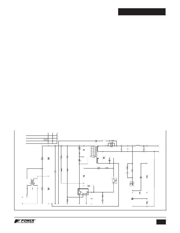
�TOP264-271�
�Very� Low� No-Load,� High� Efficiency,� 30� W,� Universal�
�Input,� Open� Frame,� Power� Supply�
�The� circuit� shown� in� Figure� 26� below� shows� an� 85� VAC� to�
�265� VAC� input,� 12� V,� 2.5� A� output� power� supply.� The� goals� of�
�the� design� were� highest� full� load� efficiency,� average� efficiency�
�(average� of� 25%,� 50%,� 75%� and� 100%� load� points),� very� low� no-�
�load� consumption.� Additional� requirements� included� latching�
�output� overvoltage� shutdown� and� compliance� to� safety� agency�
�limited� power� source� (LPS)� limits.� Actual� efficiency� and� no-load�
�performance� is� summarized� in� the� table� shown� in� the� schematic�
�which� easily� exceed� current� energy� efficiency� requirements.�
�In� order� to� meet� these� design� goals� the� following� key� design�
�decisions� were� made.�
�PI� Part� Selection�
�? � Ambient� of� 40� °C� allowed� one� device� size� smaller� than�
�indicated� by� the� power� table�
�The� device� selected� for� this� design� was� based� on� the� 85-265� VAC,�
�Open� Frame,� PCB� heat� sinking� column� of� power� table� (Table� 1).�
�One� device� size� smaller� was� selected� (TOP266V� vs� TOP267V)�
�due� to� the� ambient� specification� of� 40� °C� (vs� the� 50°C� assumed�
�in� the� power� table)� and� the� optimum� PCB� area� and� layout� for�
�the� device� heat� sink.� The� subsequent� thermal� and� efficiency�
�data� confirmed� this� choice.� The� maximum� device� temperature�
�was� 107°C� at� full� load,� 40� °C,� 85� VAC,� 47� Hz� (worst� case�
�conditions)� and� average� efficiency� exceeded� 83%� ENERGY�
�STAR� and� EuP� Tier� 2� requirements.�
�Transformer� Core� Selection�
�? � 132� kHz� switching� frequency� allowed� the� selection� of� smaller�
�core� for� lower� cost�
�The� size� of� the� magnetic� core� is� a� function� of� the� switching�
�frequency.� The� choice� of� the� higher� switching� frequency� of�
�132� kHz� allowed� for� the� use� of� a� smaller� core� size.� The� higher�
�switching� frequency� does� not� negatively� impact� the� efficiency� in�
�TOPSwitch-JX� designs� due� its� small� drain� to� source� capacitance�
�(C� OSS� )� as� compared� to� that� of� discrete� MOSFETs.�
�Line� Sense� Resistor� Values�
�? � Increasing� line� sensing� resistance� from� 4� M� W� to� 10.2� M� W� to�
�reduce� no-load� input� power� dissipation� by� 16� mW�
�Line� sensing� is� provided� by� resistors� R1� and� R2� and� sets� the�
�line� undervoltage� and� overvoltage� thresholds.� The� combined�
�value� of� these� resistors� was� increased� from� the� standard� 4� M� W�
�to� 10.2� M� W� .� This� reduces� the� current� into� the� V� pin,� and�
�therefore� contribution� to� no-load� input� power,� from� ~26� mW� to� ~�
�10� mW.� To� compensate� the� resultant� change� in� the� UV� threshold�
�resistor� R12� was� added� between� the� CONTROL� and� VOLTAGE-�
�MONITOR� pins.� This� adds� a� DC� current� equal� to� ~16� m� A� into�
�the� V� pin,� requiring� only� 9� m� A� to� be� provided� via� R1� and� R2� to�
�reach� the� V� pin� UV� threshold� current� of� 25� m� A� and� setting� the�
�UV� threshold� to� approximately� 95� VDC.�
�This� technique� does� effectively� disable� the� line� OV� feature� as�
�the� resultant� OV� threshold� is� raised� from� ~450� VDC� to� ~980� VDC.�
�However� in� this� design� there� was� no� impact� as� the� value� of�
�input� capacitance� (C3)� was� sufficient� to� allow� the� design� to�
�withstand� differential� line� surges� greater� than� 1� kV� without� the�
�peak� drain� voltage� reaching� the� BV� DSS� rating� of� U1.�
�Specific� guidelines� and� detailed� calculations� for� the� value� of� R12�
�may� be� found� in� the� TOPSwitch-JX� Application� Note.�
�Input� Voltage� (VAC)�
�85�
�115�
�230�
�Full� Load� Ef?ciency� (%)�
�Average� Ef?ciency� (%)�
�81.25� 83.94� 86.21�
�84.97� 85.13�
�C11�
�1� nF�
�250� VAC�
�C12�
�1� nF� R17�
�200� V� 22� ?�
�No-load� Input� Power� (mW)�
�60.8�
�61.98� 74.74�
�VR1�
�P6KE180A�
�6�
�7,8�
�C14�
�680� μ� F�
�25� V�
�C15�
�680� μ� F�
�25� V�
�L2�
�3.3� μ� H�
�C16�
�100� μ� F�
�25� V�
�12� V,� 2.5� A�
�25� V�
�D1�
�1N4007�
�D2�
�1N4007�
�R1�
�5.1� M� ?�
�R3�
�10� M� ?�
�R5�
�10� k� ?�
�1/2� W�
�D5�
�FR107�
�C4�
�4.7� nF�
�1� kV�
�4�
�NC� NC�
�D8,9�
�SB560�
�11,12�
�C7�
�47� μ� F�
�1�
�D7�
�BAV21WS-�
�2� 7-F�
�RTN�
�L1�
�14� mH�
�D3�
�1N4007�
�C3�
�82� μ� F�
�400� V�
�D4�
�1N4007�
�R2�
�5.1� M� ?�
�R4�
�10� M� ?�
�D�
�V�
�D6�
�BAV19WS�
�R12�
�191� k� ?�
�1%�
�T1�
�EF25�
�VR3�
�ZMM5245B-7�
�R9�
�10� ?�
�U2B�
�LTV817D�
�R18�
�110� ?�
�C18�
�47� nF�
�50� V�
�R19�
�470� ?�
�D10�
�LL4148�
�U2A�
�LTV817D�
�R21�
�86.6� k� ?�
�1%�
�L�
�N�
�F1�
�3.15� A�
�85� -� 264�
�VAC�
�C1�
�100� nF�
�275� VAC�
�R15�
�14.3� k� ?�
�1%�
�TOPSwitch-JX�
�U1�
�TOP266VG�
�S�
�CONTROL�
�X� F�
�C�
�C9�
�100� nF�
�50� V�
�R16�
�6.8� ?�
�1/8� W�
�C10�
�47� μ� F�
�25� V�
�C20�
�33� nF�
�50� V�
�U3�
�LMV431A�
�1%�
�R23�
�10� k� ?�
�1%�
�PI-5775-030810�
�Figure� 26.� Schematic� of� High� Efficiency� 12� V,� 30� W,� Universal� Input� Flyback� Supply� With� Very� Low� No-load.�
�17�
�www.powerint.com�
�Rev.� E� 08/12�
�相关PDF资料 |
PDF描述 |
|---|---|
| EMA43DRMH | CONN EDGECARD 86POS .125 SQ WW |
| TOP249FN | IC OFFLINE SWIT UVLO HV TO262 |
| 172-E15-202R021 | CONN DB15 FEMALE SLD CUP TIN |
| MIC39150-1.8BU TR | IC REG LDO 1.8V 1.5A TO-263 |
| TOP248FN | IC OFFLINE SWIT UVLO HV TO262 |
相关代理商/技术参数 |
参数描述 |
|---|---|
| TOP271EG/VG | 制造商:POWERINT 制造商全称:Power Integrations, Inc. 功能描述:Integrated Off-Line Switcher with EcoSmart Technology for Highly Efficient Power Supplies |
| TOP271EG-TL | 制造商:POWERINT 制造商全称:Power Integrations, Inc. 功能描述:Integrated Off-Line Switcher with EcoSmart Technology for Highly Efficient Power Supplies |
| TOP271KG | 功能描述:交流/直流开关转换器 Int Off-Line Switchr EcoSmart,66W/102W RoHS:否 制造商:STMicroelectronics 输出电压:800 V 输入/电源电压(最大值):23.5 V 输入/电源电压(最小值):11.5 V 开关频率:115 kHz 电源电流:1.6 mA 工作温度范围:- 40 C to + 150 C 安装风格:SMD/SMT 封装 / 箱体:SSO-10 封装:Reel |
| TOP271KG-TL | 功能描述:交流/直流开关转换器 Int Off-Line Switchr EcoSmart,66W/102W RoHS:否 制造商:STMicroelectronics 输出电压:800 V 输入/电源电压(最大值):23.5 V 输入/电源电压(最小值):11.5 V 开关频率:115 kHz 电源电流:1.6 mA 工作温度范围:- 40 C to + 150 C 安装风格:SMD/SMT 封装 / 箱体:SSO-10 封装:Reel |
| TOP271VG | 功能描述:交流/直流开关转换器 Int Off-Line Switchr 177W/244W RoHS:否 制造商:STMicroelectronics 输出电压:800 V 输入/电源电压(最大值):23.5 V 输入/电源电压(最小值):11.5 V 开关频率:115 kHz 电源电流:1.6 mA 工作温度范围:- 40 C to + 150 C 安装风格:SMD/SMT 封装 / 箱体:SSO-10 封装:Reel |
发布紧急采购,3分钟左右您将得到回复。