- 您现在的位置:买卖IC网 > PDF目录10951 > TP3054WM/NOPB (National Semiconductor)IC FILTER ENHANCE INTERFC 16SOIC PDF资料下载
参数资料
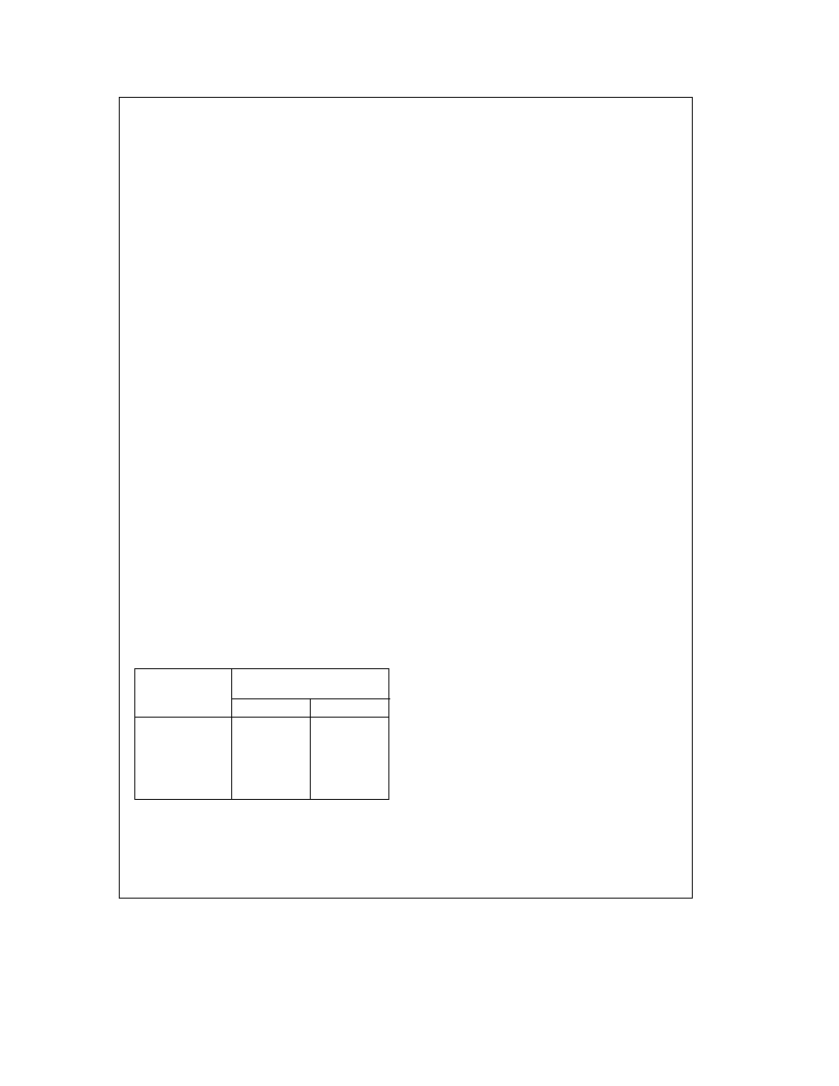
| 型号: | TP3054WM/NOPB |
| 厂商: | National Semiconductor |
| 文件页数: | 13/18页 |
| 文件大小: | 0K |
| 描述: | IC FILTER ENHANCE INTERFC 16SOIC |
| 标准包装: | 45 |
| 系列: | COMBO® |
| 类型: | PCM 编解码器/滤波器 |
| 数据接口: | 串行 |
| ADC / DAC 数量: | 1 / 1 |
| 三角积分调变: | 无 |
| 电压 - 电源,模拟: | ±5V |
| 电压 - 电源,数字: | ±5V |
| 工作温度: | -25°C ~ 125°C |
| 安装类型: | 表面贴装 |
| 封装/外壳: | 16-SOIC(0.295",7.50mm 宽) |
| 供应商设备封装: | 16-SOIC W |
| 包装: | 管件 |
| 产品目录页面: | 1276 (CN2011-ZH PDF) |
| 其它名称: | *TP3054WM *TP3054WM/NOPB TP3054WM |
Functional Description
POWER-UP
When power is first applied power-on reset circuitry initializ-
es the COMBO and places it into a power-down state All
non-essential circuits are deactivated and the DX and VFRO
outputs are put in high impedance states To power-up the
device a logical low level or clock must be applied to the
MCLKR PDN pin and FSX andor FSR pulses must be pres-
ent Thus 2 power-down control modes are available The
first is to pull the MCLKR PDN pin high the alternative is to
hold both FSX and FSR inputs continuously lowthe device
will power-down approximately 1 ms after the last FSX or
FSR pulse Power-up will occur on the first FSX or FSR
pulse The TRI-STATE PCM data output DX will remain in
the high impedance state until the second FSX pulse
SYNCHRONOUS OPERATION
For synchronous operation the same master clock and bit
clock should be used for both the transmit and receive di-
rections In this mode a clock must be applied to MCLKX
and the MCLKR PDN pin can be used as a power-down
control A low level on MCLKR PDN powers up the device
and a high level powers down the device In either case
MCLKX will be selected as the master clock for both the
transmit and receive circuits A bit clock must also be ap-
plied to BCLKX and the BCLKR CLKSEL can be used to
select the proper internal divider for a master clock of 1536
MHz 1544 MHz or 2048 MHz For 1544 MHz operation
the device automatically compensates for the 193rd clock
pulse each frame
With a fixed level on the BCLKR CLKSEL pin BCLKX will be
selected as the bit clock for both the transmit and receive
directions Table 1 indicates the frequencies of operation
which can be selected depending on the state of BCLKR
CLKSEL In this synchronous mode the bit clock BCLKX
may be from 64 kHz to 2048 MHz but must be synchro-
nous with MCLKX
Each FSX pulse begins the encoding cycle and the PCM
data from the previous encode cycle is shifted out of the
enabled DX output on the positive edge of BCLKX After 8
bit clock periods the TRI-STATE DX output is returned to a
high impedance state With an FSR pulse PCM data is
latched via the DR input on the negative edge of BCLKX (or
BCLKR if running) FSX and FSR must be synchronous with
MCLKXR
TABLE I Selection of Master Clock Frequencies
BCLKR CLKSEL
Master Clock
Frequency Selected
TP3057
TP3054
Clocked
2048 MHz
1536 MHz or
1544 MHz
0
1536 MHz or
2048 MHz
1544 MHz
1
2048 MHz
1536 MHz or
1544 MHz
ASYNCHRONOUS OPERATION
For asynchronous operation separate transmit and receive
clocks may be applied
MCLKX and MCLKR must be
2048 MHz for the TP3057 or 1536 MHz 1544 MHz for the
TP3054 and need not be synchronous For best transmis-
sion performance however MCLKR should be synchronous
with MCLKX which is easily achieved by applying only static
logic levels to the MCLKR PDN pin This will automatically
connect MCLKX to all internal MCLKR functions (see Pin
Description) For 1544 MHz operation the device automati-
cally compensates for the 193rd clock pulse each frame
FSX starts each encoding cycle and must be synchronous
with MCLKX and BCLKX FSR starts each decoding cycle
and must be synchronous with BCLKR BCLKR must be a
clock the logic levels shown in Table 1 are not valid in
asynchronous mode BCLKX and BCLKR may operate from
64 kHz to 2048 MHz
SHORT FRAME SYNC OPERATION
The COMBO can utilize either a short frame sync pulse or a
long frame sync pulse Upon power initialization the device
assumes a short frame mode In this mode both frame sync
pulses FSX and FSR must be one bit clock period long
with timing relationships specified in
Figure 2 With FSX high
during a falling edge of BCLKX the next rising edge of
BCLKX enables the DX TRI-STATE output buffer which will
output the sign bit The following seven rising edges clock
out the remaining seven bits and the next falling edge dis-
ables the DX output With FSR high during a falling edge of
BCLKR (BCLKX in synchronous mode) the next falling edge
of BCLKR latches in the sign bit The following seven falling
edges latch in the seven remaining bits All four devices
may utilize the short frame sync pulse in synchronous or
asynchronous operating mode
LONG FRAME SYNC OPERATION
To use the long frame mode both the frame sync pulses
FSX and FSR must be three or more bit clock periods long
with timing relationships specified in
Figure 3 Based on the
transmit frame sync FSX the COMBO will sense whether
short or long frame sync pulses are being used For 64 kHz
operation the frame sync pulse must be kept low for a mini-
mum of 160 ns The DX TRI-STATE output buffer is enabled
with the rising edge of FSX or the rising edge of BCLKX
whichever comes later and the first bit clocked out is the
sign bit The following seven BCLKX rising edges clock out
the remaining seven bits The DX output is disabled by the
falling BCLKX edge following the eighth rising edge or by
FSX going low whichever comes later A rising edge on the
receive frame sync pulse FSR will cause the PCM data at
DR to be latched in on the next eight falling edges of BCLKR
(BCLKX in synchronous mode) All four devices may utilize
the long frame sync pulse in synchronous or asynchronous
mode
In applications where the LSB bit is used for signalling with
FSR two bit clock periods long the decoder will interpret the
lost LSB as ‘‘
’’ to minimize noise and distortion
3
相关PDF资料 |
PDF描述 |
|---|---|
| MK51DN256ZCMD10 | IC ARM CORTEX MCU 256KB 144BGA |
| VI-26T-IY-F4 | CONVERTER MOD DC/DC 6.5V 50W |
| MC9S12XHZ512CAL | IC MCU 16BIT 512 FLASH 112-LQFP |
| VI-26T-IY-F1 | CONVERTER MOD DC/DC 6.5V 50W |
| VI-26R-IY-F2 | CONVERTER MOD DC/DC 7.5V 50W |
相关代理商/技术参数 |
参数描述 |
|---|---|
| TP3054WMX | 制造商:NSC 制造商全称:National Semiconductor 功能描述:Engineering Project Manager |
| TP3054WM-X | 功能描述:接口—CODEC RoHS:否 制造商:Texas Instruments 类型: 分辨率: 转换速率:48 kSPs 接口类型:I2C ADC 数量:2 DAC 数量:4 工作电源电压:1.8 V, 2.1 V, 2.3 V to 5.5 V 最大工作温度:+ 85 C 安装风格:SMD/SMT 封装 / 箱体:DSBGA-81 封装:Reel |
| TP3054WM-X/63 | 功能描述:接口—CODEC RoHS:否 制造商:Texas Instruments 类型: 分辨率: 转换速率:48 kSPs 接口类型:I2C ADC 数量:2 DAC 数量:4 工作电源电压:1.8 V, 2.1 V, 2.3 V to 5.5 V 最大工作温度:+ 85 C 安装风格:SMD/SMT 封装 / 箱体:DSBGA-81 封装:Reel |
| TP3054WM-X/63SN | 功能描述:接口—CODEC RoHS:否 制造商:Texas Instruments 类型: 分辨率: 转换速率:48 kSPs 接口类型:I2C ADC 数量:2 DAC 数量:4 工作电源电压:1.8 V, 2.1 V, 2.3 V to 5.5 V 最大工作温度:+ 85 C 安装风格:SMD/SMT 封装 / 箱体:DSBGA-81 封装:Reel |
| TP3054WMX/NOPB | 功能描述:接口—CODEC RoHS:否 制造商:Texas Instruments 类型: 分辨率: 转换速率:48 kSPs 接口类型:I2C ADC 数量:2 DAC 数量:4 工作电源电压:1.8 V, 2.1 V, 2.3 V to 5.5 V 最大工作温度:+ 85 C 安装风格:SMD/SMT 封装 / 箱体:DSBGA-81 封装:Reel |
发布紧急采购,3分钟左右您将得到回复。