- 您现在的位置:买卖IC网 > PDF目录98276 > TPA6203A1GQV (TEXAS INSTRUMENTS INC) 1.25 W, 1 CHANNEL, AUDIO AMPLIFIER, PBGA8 PDF资料下载
参数资料
| 型号: | TPA6203A1GQV |
| 厂商: | TEXAS INSTRUMENTS INC |
| 元件分类: | 音频/视频放大 |
| 英文描述: | 1.25 W, 1 CHANNEL, AUDIO AMPLIFIER, PBGA8 |
| 封装: | PLASTIC, BGA-8 |
| 文件页数: | 5/19页 |
| 文件大小: | 214K |
| 代理商: | TPA6203A1GQV |
TPA6203A1
SLOS364 – MARCH 2002
www.ti.com
13
is slewing up, the other side is slewing down, and vice
versa. This in effect doubles the voltage swing on the load
as compared to a ground referenced load. Plugging 2
×
VO(PP) into the power equation, where voltage is squared,
yields 4
× the output power from the same supply rail and
load impedance (see equation 4).
V
(rms) +
V
O(PP)
22
Power
+
V
(rms)
2
R
L
RL
2x VO(PP)
VO(PP)
–VO(PP)
VDD
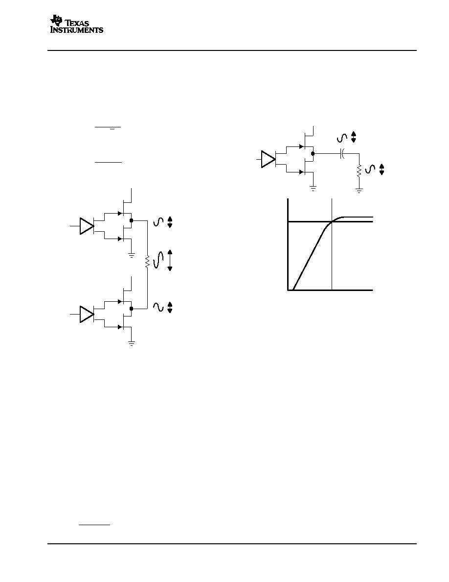
Figure 32. Differential Output Configuration
In a typical wireless handset operating at 3.6 V, bridging
raises the power into an 8-
speaker from a singled-ended
(SE, ground reference) limit of 200 mW to 800 mW. In
sound power that is a 6-dB improvement—which is
loudness that can be heard. In addition to increased power
there are frequency response concerns. Consider the
single-supply SE configuration shown in Figure 33. A
coupling capacitor is required to block the dc offset voltage
from reaching the load. This capacitor can be quite large
(approximately 33
F to 1000 F) so it tends to be
expensive, heavy, occupy valuable PCB area, and have
the
additional
drawback
of
limiting
low-frequency
performance of the system. This frequency limiting effect
is due to the high pass filter network created with the
speaker impedance and the coupling capacitance and is
calculated with equation 5.
fc +
1
2
pR
L
C
For example, a 68-
F capacitor with an 8- speaker would
attenuate low frequencies below 293 Hz. The BTL
configuration cancels the dc offsets, which eliminates the
need
for
the
blocking
capacitors.
Low-frequency
performance is then limited only by the input network and
speaker response. Cost and PCB space are also
minimized by eliminating the bulky coupling capacitor.
RL
CC
VO(PP)
VDD
–3 dB
fc
Figure 33. Single-Ended Output and Frequency
Response
Increasing power to the load does carry a penalty of
increased internal power dissipation. The increased
dissipation is understandable considering that the BTL
configuration produces 4
× the output power of the SE
configuration.
FULLY DIFFERENTIAL AMPLIFIER
EFFICIENCY AND THERMAL INFORMATION
Class-AB amplifiers are known to be inefficient. The
primary cause of these inefficiencies is voltage drop
across the output stage transistors. There are two
components of the internal voltage drop. One is the
headroom or dc voltage drop that varies inversely to output
power. The second component is due to the sinewave
nature of the output. The total voltage drop can be
calculated by subtracting the RMS value of the output
voltage from VDD. The internal voltage drop multiplied by
the average value of the supply current, IDD(avg),
determines the internal power dissipation of the amplifier.
An easy-to-use equation to calculate efficiency starts out
as being equal to the ratio of power from the power supply
to the power delivered to the load. To accurately calculate
the RMS and average values of power in the load and in
the amplifier, the current and voltage waveform shapes
must first be understood (see Figure 34).
(4)
(5)
相关PDF资料 |
PDF描述 |
|---|---|
| TPA6203AIDGN | 1.25 W, 1 CHANNEL, AUDIO AMPLIFIER, PDSO8 |
| TPA6203AIDRB | 1.25 W, 1 CHANNEL, AUDIO AMPLIFIER, PDSO8 |
| TPA6204A1DGN | 1.7 W, 1 CHANNEL, AUDIO AMPLIFIER, PDSO8 |
| TPA6205A1DGN | 1.25 W, 1 CHANNEL, AUDIO AMPLIFIER, PDSO8 |
| TPA6205A1DRBR | 1.25 W, 1 CHANNEL, AUDIO AMPLIFIER, PDSO8 |
相关代理商/技术参数 |
参数描述 |
|---|---|
| TPA6203A1GQVR | 功能描述:音频放大器 Mono Fully Diff Class-AB RoHS:否 制造商:STMicroelectronics 产品:General Purpose Audio Amplifiers 输出类型:Digital 输出功率: THD + 噪声: 工作电源电压:3.3 V 电源电流: 最大功率耗散: 最大工作温度: 安装风格:SMD/SMT 封装 / 箱体:TQFP-64 封装:Reel |
| TPA6203A1ZQVR | 功能描述:音频放大器 Mono Fully Diff Class-AB RoHS:否 制造商:STMicroelectronics 产品:General Purpose Audio Amplifiers 输出类型:Digital 输出功率: THD + 噪声: 工作电源电压:3.3 V 电源电流: 最大功率耗散: 最大工作温度: 安装风格:SMD/SMT 封装 / 箱体:TQFP-64 封装:Reel |
| TPA6203A1ZQVRG1 | 功能描述:音频放大器 1.25W Mon,Fully Diff Class-AB Audio Amp RoHS:否 制造商:STMicroelectronics 产品:General Purpose Audio Amplifiers 输出类型:Digital 输出功率: THD + 噪声: 工作电源电压:3.3 V 电源电流: 最大功率耗散: 最大工作温度: 安装风格:SMD/SMT 封装 / 箱体:TQFP-64 封装:Reel |
| TPA6204A1 | 制造商:TI 制造商全称:Texas Instruments 功能描述:1.7W MONO FULLY DIFFERENTIAL AUDIO POWER AMPLIFIER |
| TPA6204A1_07 | 制造商:TI 制造商全称:Texas Instruments 功能描述:1.7W MONO FULLY DIFFERENTIAL AUDIO POWER AMPLIFIER |
发布紧急采购,3分钟左右您将得到回复。