- 您现在的位置:买卖IC网 > PDF目录69509 > TPS40130RHBRG4 (TEXAS INSTRUMENTS INC) SWITCHING CONTROLLER, 1200 kHz SWITCHING FREQ-MAX, PQCC32 PDF资料下载
参数资料
| 型号: | TPS40130RHBRG4 |
| 厂商: | TEXAS INSTRUMENTS INC |
| 元件分类: | 稳压器 |
| 英文描述: | SWITCHING CONTROLLER, 1200 kHz SWITCHING FREQ-MAX, PQCC32 |
| 封装: | GREEN, PLASTIC, QFN-32 |
| 文件页数: | 36/38页 |
| 文件大小: | 950K |
| 代理商: | TPS40130RHBRG4 |
第1页第2页第3页第4页第5页第6页第7页第8页第9页第10页第11页第12页第13页第14页第15页第16页第17页第18页第19页第20页第21页第22页第23页第24页第25页第26页第27页第28页第29页第30页第31页第32页第33页第34页第35页当前第36页第37页第38页
www.ti.com
1
2
3
4
5
6
7
8
9
10
11
12
13
14
15
30
29
28
27
26
25
24
23
22
21
20
19
18
17
16
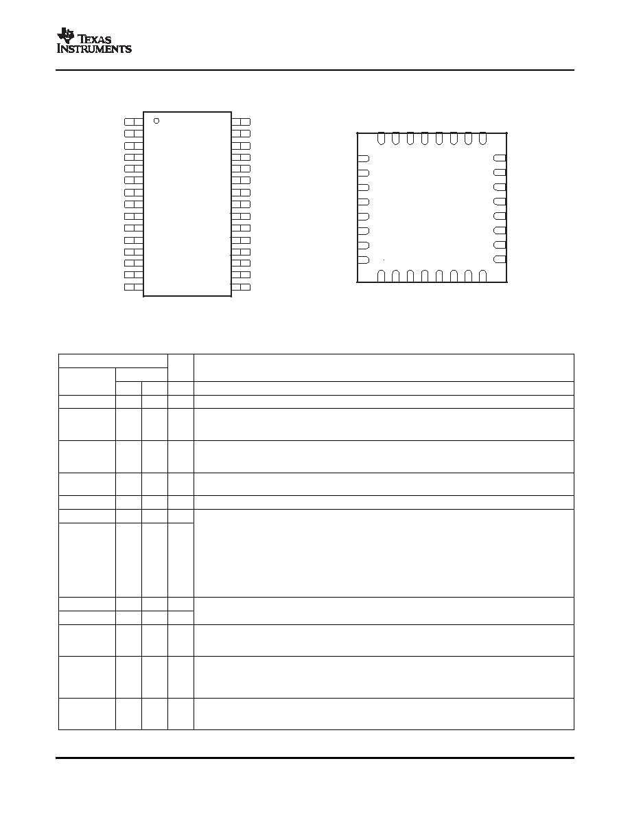
LDRV1
VIN5
SW1
HDRV1
BOOT1
OVSET
VOUT
GSNS
DIFFO
CS1
CSRT1
COMP
VREF
DROOP
FB
PGND
LDRV2
SW2
HDRV2
BOOT2
SS
UVLO
BP5
AGND
CS2
CSRT2
RT
PGOOD
ILIM
EN/SYNC
DBT PACKAGE
(TOP VIEW)
RHB PACKAGE
(TOP VIEW)
32 31 30
29 28 27 26 25
24
23
22
21
20
19
18
17
9 10 11 12 13
15 16
BOOT1
OVSET
VOUT
GSNS
DIFFO
CS1
CSRT1
NC
BOOT2
SS
UVLO
BP5
AGND
CS2
CSRT2
COMP
HDR
V1
SW1
VIN5
LDR
V1
PGND
LDR
V2
SW2
HDR
V2
VREF
DROOP
FB
EN/SYNC
ILIM
PGOOD
R
T
14
1
2
3
4
5
6
7
8
SLUS602B – JUNE 2004 – REVISED SEPTEMBER 2005
Terminal Functions
TERMINAL
I/O
DESCRIPTION
NO.
NAME
RHB
DBT
AGND
19
22
-
Low noise ground connection to the device.
Provides a bootstrapped supply for the high-side FET driver for PWM1, enabling the gate of the
BOOT1
1
5
I
high-side FET to be driven above the input supply rail. Connect a capacitor from this pin to SW1 pin
and a Schottky diode from this pin to VIN5.
Provides a bootstrapped supply for the high-side FET driver for PWM2, enabling the gate of the
BOOT2
23
26
I
high-side FET to be driven above the input supply rail. Connect a capacitor from this pin to SW2 pin
and a Schottky diode from this pin to VIN5.
Filtered input from the VIN5 pin. A 10-
resistor should be connected between VIN5 and BP5 and a
BP5
20
23
O
1.0-F ceramic capacitor should be connected from this pin to ground.
COMP
9
12
O
Output of the error amplifier. The voltage at this pin determines the duty cycle for the PWM.
CS1
6
10
I
These pins are used to sense the inductor phase current. Inductor current can be sensed with an
external current sense resistor or by using an external R-C circuit and the inductor's DC resistance.
The traces for these signals must be connected directly at the current sense element. See Layout
Guidelines for more information. After the device is enabled and prior to the device starting (during the
first 32 clock cycles), a 5-A current flows out of these pins. The current flows through the external
CS2
18
21
I
components: current sense resistor, RCS, the output inductor and the output capacitor(s) to ground. If
the voltage on the CS1, and CS2 pins exceed 0.2 V (resistance greater than 40 k
), a fault is
declared and the device does not start. This is a fault detection feature that insures the output
inductor, current sense resistor and output capacitors are installed properly on the board.
CSRT1
7
11
O
Return point of current sense voltage. The traces for these signals must be connected directly at the
current sense element. See Layout Guidelines for more information.
CSRT2
17
20
O
Output of the differential amplifier. The voltage at this pin represents the true output voltage without IR
DIFFO
5
9
O
drops that result from high-current in the PCB traces. The VOUT and GSNS pins must be connected
directly at the point of load where regulation is required. See Layout Guidelines for more information.
This is the input to the non-inverting input of the Error Amplifier. This pin is normally connected to the
VREF pin and is the voltage that the feedback loop regulates to. This pin is also used to program
DROOP
11
14
I
droop function. A resistor between this pin and the VREF pin sets the desired droop value. The value
of the DROOP resistor is described in Equation 22.
A logic high signal on this input enables the controller operation. A pulsing signal to this pin
EN/SYNC
13
16
I
synchronizes the rising edge of SW to the falling edge of an external clock source. These pulses must
be greater than 8.2 times the free running frequency of the main oscillator set by the RT resistor.
7
相关PDF资料 |
PDF描述 |
|---|---|
| TPS40130RHB | SWITCHING CONTROLLER, 1200 kHz SWITCHING FREQ-MAX, PQCC32 |
| TPS40140RHHTG4 | 0.1 A DUAL SWITCHING CONTROLLER, 1000 kHz SWITCHING FREQ-MAX, PQCC36 |
| TPS40140RHHT | 0.1 A DUAL SWITCHING CONTROLLER, 1000 kHz SWITCHING FREQ-MAX, PQCC36 |
| TPS40140RHHR | 0.1 A DUAL SWITCHING CONTROLLER, 1000 kHz SWITCHING FREQ-MAX, PQCC36 |
| TPS40180RGERG4 | 0.05 A SWITCHING CONTROLLER, 1000 kHz SWITCHING FREQ-MAX, PQCC24 |
相关代理商/技术参数 |
参数描述 |
|---|---|
| TPS40130RHBT | 功能描述:DC/DC 开关控制器 2-Ch Multiphase Buck DC/DC w/Int Drvr RoHS:否 制造商:Texas Instruments 输入电压:6 V to 100 V 开关频率: 输出电压:1.215 V to 80 V 输出电流:3.5 A 输出端数量:1 最大工作温度:+ 125 C 安装风格: 封装 / 箱体:CPAK |
| TPS40130RHBTG4 | 功能描述:DC/DC 开关控制器 2-Ch Multiphase Buck DC/DC w/Int Drvr RoHS:否 制造商:Texas Instruments 输入电压:6 V to 100 V 开关频率: 输出电压:1.215 V to 80 V 输出电流:3.5 A 输出端数量:1 最大工作温度:+ 125 C 安装风格: 封装 / 箱体:CPAK |
| TPS40131 | 制造商:TI 制造商全称:Texas Instruments 功能描述:TWO-PHASE, SYNCHRONOUS BUCK CONTROLLER WITH INTEGRATED MOSFET DRIVERS |
| TPS40131EVM | 功能描述:电源管理IC开发工具 TPS40131 Eval Mod RoHS:否 制造商:Maxim Integrated 产品:Evaluation Kits 类型:Battery Management 工具用于评估:MAX17710GB 输入电压: 输出电压:1.8 V |
| TPS40131RHBR | 功能描述:DC/DC 开关控制器 2-Ph Synch Buck Cntr RoHS:否 制造商:Texas Instruments 输入电压:6 V to 100 V 开关频率: 输出电压:1.215 V to 80 V 输出电流:3.5 A 输出端数量:1 最大工作温度:+ 125 C 安装风格: 封装 / 箱体:CPAK |
发布紧急采购,3分钟左右您将得到回复。