- 您现在的位置:买卖IC网 > PDF目录14264 > TPS51317RGBR (Texas Instruments)IC REG BUCK SYNC ADJ 6A 20VQFN PDF资料下载
参数资料
| 型号: | TPS51317RGBR |
| 厂商: | Texas Instruments |
| 文件页数: | 11/28页 |
| 文件大小: | 0K |
| 描述: | IC REG BUCK SYNC ADJ 6A 20VQFN |
| 标准包装: | 3,000 |
| 系列: | D-Cap+™ |
| 类型: | 降压(降压) |
| 输出类型: | 可调式 |
| 输出数: | 1 |
| 输出电压: | 0.6 V ~ 2 V |
| 输入电压: | 4.5 V ~ 6.5 V |
| PWM 型: | 混合物 |
| 频率 - 开关: | 800kHz,1MHz,1.2MHz,1.5MHz |
| 电流 - 输出: | 6A |
| 同步整流器: | 是 |
| 工作温度: | -40°C ~ 85°C |
| 安装类型: | 表面贴装 |
| 封装/外壳: | 20-VFQFN 裸露焊盘 |
| 包装: | 带卷 (TR) |
| 供应商设备封装: | 20-VQFN(3.5x4.0) |
第1页第2页第3页第4页第5页第6页第7页第8页第9页第10页当前第11页第12页第13页第14页第15页第16页第17页第18页第19页第20页第21页第22页第23页第24页第25页第26页第27页第28页
�� ��
��
��V� OUT�
�V� IN� SW�
��PWM� Frequency� and� Adaptive� on� Time� Control�
��1�
�t� ON� =� ′�
�f�
�where�
�SLUSAH9� –� MARCH� 2011�
�?�
�f� SW� is� the� frequency� selected� by� the� connection� of� the� MODE� pin�
�(1)�
�The� on-time� pulse� is� sent� to� the� top� FET.� The� inductor� current� and� the� current� feedback� rises� to� peak� value.�
�Each� ON� pulse� is� latched� to� prevent� double� pulsing.� Switching� frequency� settings� are� shown� in� .�
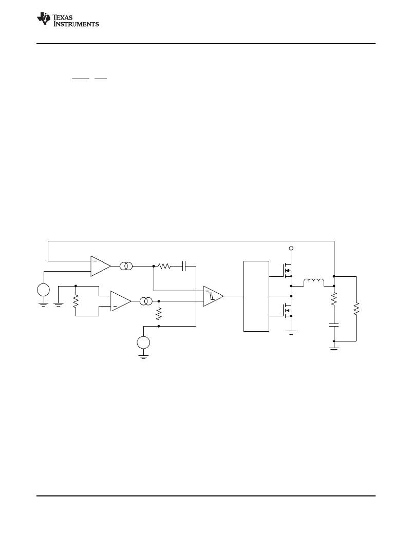
�Non-Droop� Configuration�
�The� TPS51317� can� be� configured� as� a� non-droop� solution.� The� benefit� of� a� non-droop� approach� is� that� load�
�regulation� is� flat,� therefore,� in� a� system� where� tight� DC� tolerance� is� desired,� the� non-droop� approach� is�
�recommended.� For� the� Intel� system� agent� application,� non-droop� is� recommended� as� the� standard� configuration.�
�The� non-droop� approach� can� be� implemented� by� connecting� a� resistor� and� a� capacitor� between� the� COMP� and�
�the� VREF� pins.� The� purpose� of� the� type� II� compensation� is� to� obtain� high� DC� feedback� gain� while� minimizing� the�
�phase� delay� at� unity� gain� cross� over� frequency� of� the� converter.�
�The� value� of� the� resistor� (R� C� )� can� be� calculated� using� the� desired� unity� gain� bandwidth� of� the� converter,� and� the�
�value� of� the� capacitor� (C� C� )� can� be� calculated� by� knowing� where� the� zero� location� is� desired.� An� application� tool�
�that� calculates� these� values� is� available� from� your� local� TI� Field� Application� Engineer.�
��G� MV� =� 1� mS�
�R� C�
�C� C�
�+�
�V� SLEW�
�+�
�L� OUT�
�–�
�R� DS(on)�
�+�
�G� MC� =� 1� mS�
�+�
�PWM�
�Driver�
�ESR�
�+�
�–�
�R� LOAD�
�8� k� W�
�VREF�
�Comparator�
�C� OUT�
�R� OUT�
�UDG-10190�
�Figure� 4.� Non-Droop� Mode� Basic� Implementation�
��Figure� 6� shows� the� transient� response� of� TPS51317� using� non-droop� configuration,� where� C� OUT� =� 6� x� 22� μ� F.� The�
�applied� step� load� is� from� 0� A� to� 3� A.�
�Copyright� ?� 2011,� Texas� Instruments� Incorporated�
�Product� Folder� Link(s):� TPS51317�
��11�
�相关PDF资料 |
PDF描述 |
|---|---|
| VE-BVR-EX-F3 | CONVERTER MOD DC/DC 7.5V 75W |
| RCA30DRSN-S288 | CONN EDGECARD 60POS .125 EXTEND |
| VE-BVR-EX-F2 | CONVERTER MOD DC/DC 7.5V 75W |
| HM50-3R9KLF | MINIATURE POWER INDUCTORS AXIAL |
| RCA30DRSD-S288 | CONN EDGECARD 60POS .125 EXTEND |
相关代理商/技术参数 |
参数描述 |
|---|---|
| TPS51317RGBT | 功能描述:直流/直流开关转换器 3.3V/5Vin,6A,DCAP Mode Sync Converter RoHS:否 制造商:STMicroelectronics 最大输入电压:4.5 V 开关频率:1.5 MHz 输出电压:4.6 V 输出电流:250 mA 输出端数量:2 最大工作温度:+ 85 C 安装风格:SMD/SMT |
| TPS51362RVER | 制造商:Texas Instruments 功能描述:22V INPUT, 10A INTEGRATED FET 制造商:Texas Instruments 功能描述:IC REG BUCK SYNC ADJ 10A 28VQFN |
| TPS51362RVET | 制造商:Texas Instruments 功能描述:22V INPUT, 10A INTEGRATED FET 制造商:Texas Instruments 功能描述:IC REG BUCK SYNC ADJ 10A 28VQFN |
| TPS51363 | 制造商:TI 制造商全称:Texas Instruments 功能描述:22-V Input, 8-A or 10-A Converter With Integrated FET |
| TPS51363RVER | 制造商:Texas Instruments 功能描述:Conv DC-DC Single Step Down 3V to 22V 28-Pin VQFN EP T/R 制造商:Texas Instruments 功能描述:IC REG BCK SYNC ADJ 10/8A 28VQFN |
发布紧急采购,3分钟左右您将得到回复。