- 您现在的位置:买卖IC网 > PDF目录98283 > TPS56100PWPR (TEXAS INSTRUMENTS INC) 1.4 A SWITCHING CONTROLLER, 500 kHz SWITCHING FREQ-MAX, PDSO28 PDF资料下载
参数资料
| 型号: | TPS56100PWPR |
| 厂商: | TEXAS INSTRUMENTS INC |
| 元件分类: | 稳压器 |
| 英文描述: | 1.4 A SWITCHING CONTROLLER, 500 kHz SWITCHING FREQ-MAX, PDSO28 |
| 封装: | GREEN, PLASTIC, HTSSOP-28 |
| 文件页数: | 29/30页 |
| 文件大小: | 595K |
| 代理商: | TPS56100PWPR |
第1页第2页第3页第4页第5页第6页第7页第8页第9页第10页第11页第12页第13页第14页第15页第16页第17页第18页第19页第20页第21页第22页第23页第24页第25页第26页第27页第28页当前第29页第30页
TPS56100
HIGHEFFICIENCY DSP POWER SUPPLY CONTROLLER
FOR 5V INPUT SYSTEMS
SLVS201A JUNE 1999 REVISED JULY 1999
8
POST OFFICE BOX 655303
DALLAS, TEXAS 75265
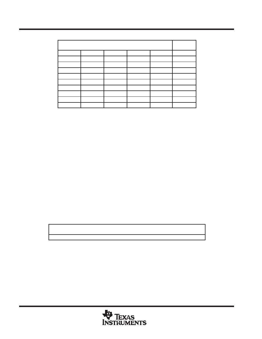
Table 1. Voltage Programming Codes (Continued)
VP TERMINALS
(0 = GND, 1 = floating or pull-up to 5 V)
VREF
VP4
VP3
VP2
VP1
VP0
(Vdc)
1
0
2.60
1
0
1
2.60
1
0
1
0
2.60
1
0
1
0
1
2.60
1
0
1
0
2.60
1
0
1
2.60
1
0
1
0
2.60
1
0
1
2.60
1
0
2.60
absolute maximum ratings over operating virtual junction temperature (unless otherwise noted)
Supply voltage range, VCC (see Note1), BIAS, DRV
0.3 V to 7 V
. . . . . . . . . . . . . . . . . . . . . . . . . . . . . . . . . . . .
Input voltage range: BOOT to DRVGND (High-side Driver ON)
0.3 V to 30 V
. . . . . . . . . . . . . . . . . . . . . . . . .
BOOT to HIGHDRV
0.3 V to 15 V
. . . . . . . . . . . . . . . . . . . . . . . . . . . . . . . . . . . . . . . . . . . .
BOOT to BOOTLO
0.3 V to 15 V
. . . . . . . . . . . . . . . . . . . . . . . . . . . . . . . . . . . . . . . . . . . . .
INHIBIT, VPx, LODRV
0.3 V to 7.3 V
. . . . . . . . . . . . . . . . . . . . . . . . . . . . . . . . . . . . . . . . . .
PWRGD, OCP
0.3 V to 7 V
. . . . . . . . . . . . . . . . . . . . . . . . . . . . . . . . . . . . . . . . . . . . . . . . .
LOHIB, LOSENSE, IOUTLO, HISENSE
0.3 V to 7 V
. . . . . . . . . . . . . . . . . . . . . . . . . . .
VSENSE
0.3 V to 5 V
. . . . . . . . . . . . . . . . . . . . . . . . . . . . . . . . . . . . . . . . . . . . . . . . . . . . . .
Voltage difference between ANAGND and DRVGND
±0.5 V
. . . . . . . . . . . . . . . . . . . . . . . . . . . . . . . . . . . . . . . . .
Output current, VREFB
0.5 mA
. . . . . . . . . . . . . . . . . . . . . . . . . . . . . . . . . . . . . . . . . . . . . . . . . . . . . . . . . . . . . . . . . . . .
Continuous total power dissipation
See Dissipation Rating Table
. . . . . . . . . . . . . . . . . . . . . . . . . . . . . . . . . . . . .
Operating virtual junction temperature range, TJ
0
°C to 125°C
. . . . . . . . . . . . . . . . . . . . . . . . . . . . . . . . . . . . . . .
Storage temperature range, Tstg
65
°C to 150°C
. . . . . . . . . . . . . . . . . . . . . . . . . . . . . . . . . . . . . . . . . . . . . . . . . . .
Lead temperature soldering 1,6 mm (1/16 inch) from case for 10 seconds
260
°C
. . . . . . . . . . . . . . . . . . . . . . .
Stresses beyond those listed under “absolute maximum ratings” may cause permanent damage to the device. These are stress ratings only, and
functional operation of the device at these or any other conditions beyond those indicated under “recommended operating conditions” is not
implied. Exposure to absolute-maximum-rated conditions for extended periods may affect device reliability.
NOTE 1: Unless otherwise specified, all voltages are with respect to ANAGND.
DISSIPATION RATING TABLE
PACKAGE
TA ≤ 25°C
POWER RATING
DERATING FACTOR
ABOVE TA = 25°C
TA = 70°C
POWER RATING
TA = 85°C
POWER RATING
PWP
1150 mW
11.5 mW/
°C
630 mW
460 mW
相关PDF资料 |
PDF描述 |
|---|---|
| TPS56100PWPRG4 | 1.4 A SWITCHING CONTROLLER, 500 kHz SWITCHING FREQ-MAX, PDSO28 |
| TPS56121DQPT | SWITCHING CONTROLLER, 1100 kHz SWITCHING FREQ-MAX, PDSO22 |
| TPS5615CPWP | SWITCHING CONTROLLER, PDSO28 |
| TPS5625CPWPR | SWITCHING CONTROLLER, PDSO28 |
| TPS56221DQPR | SWITCHING CONTROLLER, PDSO22 |
相关代理商/技术参数 |
参数描述 |
|---|---|
| TPS56100PWPRG4 | 功能描述:DC/DC 开关控制器 5B Programmable Synch Buck Cntrlr RoHS:否 制造商:Texas Instruments 输入电压:6 V to 100 V 开关频率: 输出电压:1.215 V to 80 V 输出电流:3.5 A 输出端数量:1 最大工作温度:+ 125 C 安装风格: 封装 / 箱体:CPAK |
| TPS561201DDCR | 功能描述:AUGUSTA NEXT 1A 制造商:texas instruments 系列:* 零件状态:在售 标准包装:1 |
| TPS561201DDCT | 功能描述:4.5V TO 17V INPUT, 1A SYNCHRONOU 制造商:texas instruments 系列:SWIFT?? 包装:剪切带(CT) 零件状态:在售 功能:降压 输出配置:正 拓扑:降压 输出类型:可调式 输出数:1 电压 - 输入(最小值):4.5V 电压 - 输入(最大值):17V 电压 - 输出(最小值/固定):0.76V 电压 - 输出(最大值):7V 电流 - 输出:1A 频率 - 开关:580kHz 同步整流器:是 工作温度:-40°C ~ 85°C(TA) 安装类型:表面贴装 封装/外壳:SOT-23-6 细型,TSOT-23-6 供应商器件封装:SOT-23-6 标准包装:1 |
| TPS561201EVM-896 | 功能描述:EVAIL MOD 制造商:texas instruments 系列:* 零件状态:在售 标准包装:1 |
| TPS561208DDCR | 功能描述:AUGUSTANEXT 1A 制造商:texas instruments 系列:* 零件状态:在售 标准包装:1 |
发布紧急采购,3分钟左右您将得到回复。