- 您现在的位置:买卖IC网 > PDF目录136934 > TPS62200DBVTG4 (TEXAS INSTRUMENTS INC) 0.67 A SWITCHING REGULATOR, 1500 kHz SWITCHING FREQ-MAX, PDSO5 PDF资料下载
参数资料
| 型号: | TPS62200DBVTG4 |
| 厂商: | TEXAS INSTRUMENTS INC |
| 元件分类: | 稳压器 |
| 英文描述: | 0.67 A SWITCHING REGULATOR, 1500 kHz SWITCHING FREQ-MAX, PDSO5 |
| 封装: | GREEN, PLASTIC, SOT-23, 5 PIN |
| 文件页数: | 6/23页 |
| 文件大小: | 590K |
| 代理商: | TPS62200DBVTG4 |
www.ti.com
DVout + Vout
1– Vout
Vin
L
f
1
8
Cout
f )
ESR
LAYOUT CONSIDERATIONS
VI
GND
EN
SW
FB
C1
4.7
F
L1
10
H
C2
10
F
TPS62200
VI
2.5 V 6 V
VO
1.8 V / 300 mA
R1
R2
Cff
SLVS417E – MARCH 2002 – REVISED MAY 2006
At nominal load current the device operates in PWM mode and the overall output voltage ripple is the sum of the
voltage spike caused by the output capacitor ESR plus the voltage ripple caused by charging and discharging
the output capacitor:
where the highest output voltage ripple occurs at the highest input voltage Vin.
At light load currents, the device operates in power save mode, and the output voltage ripple is independent of
the output capacitor value. The output voltage ripple is set by the internal comparator thresholds. The typical
output voltage ripple is 1% of the output voltage Vo.
Table 2. Recommended Capacitors
CAPACITOR VALUE
CASE SIZE
COMPONENT SUPPLIER
COMMENTS
4.7 F
0805
Taiyo Yuden JMK212BY475MG
Ceramic
10 F
0805
Taiyo Yuden JMK212BJ106MG
Ceramic
TDK C12012X5ROJ106K
Ceramic
10 F
1206
Taiyo Yuden JMK316BJ106KL
Ceramic
TDK C3216X5ROJ106M
22 F
1210
Taiyo Yuden JMK325BJ226MM
Ceramic
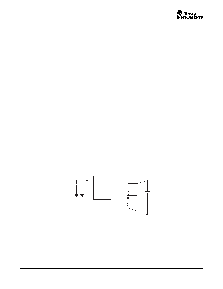
For all switching power supplies, the layout is an important step in the design, especially at high peak currents
and switching frequencies. If the layout is not carefully done, the regulator shows stability problems as well as
EMI problems.
Therefore use wide and short traces for the main current paths, as indicated in bold in Figure 17. The input
capacitor, as well as the inductor and output capacitor, should be placed as close as possible to the IC pins
The feedback resistor network must be routed away from the inductor and switch node to minimize noise and
magnetic interference. To further minimize noise from coupling into the feedback network and feedback pin, the
ground plane or ground traces must be used for shielding. This becomes very important especially at high
switching frequencies of 1 MHz.
Figure 17. Layout Diagram
14
相关PDF资料 |
PDF描述 |
|---|---|
| TPS60242DGKRG4 | 0.012 A SWITCHED CAPACITOR REGULATOR, 220 kHz SWITCHING FREQ-MAX, PDSO8 |
| TC151B3813EOA723 | 0.25 A SWITCHING REGULATOR, 50 kHz SWITCHING FREQ-MAX, PDSO8 |
| TC151A1518EOA713 | 0.25 A SWITCHING REGULATOR, 50 kHz SWITCHING FREQ-MAX, PDSO8 |
| TC151B4024EOA723 | 0.25 A SWITCHING REGULATOR, 50 kHz SWITCHING FREQ-MAX, PDSO8 |
| TC151B4724EOA713 | 0.25 A SWITCHING REGULATOR, 50 kHz SWITCHING FREQ-MAX, PDSO8 |
相关代理商/技术参数 |
参数描述 |
|---|---|
| TPS62200EVM-211 | 功能描述:电源管理IC开发工具 Adj 300-mA Step-down Conv Eval Mod RoHS:否 制造商:Maxim Integrated 产品:Evaluation Kits 类型:Battery Management 工具用于评估:MAX17710GB 输入电压: 输出电压:1.8 V |
| TPS62201DBVR | 功能描述:直流/直流开关调节器 300mA Hi-Eff Step-Down Converter RoHS:否 制造商:International Rectifier 最大输入电压:21 V 开关频率:1.5 MHz 输出电压:0.5 V to 0.86 V 输出电流:4 A 输出端数量: 最大工作温度: 安装风格:SMD/SMT 封装 / 箱体:PQFN 4 x 5 |
| TPS62201DBVRG4 | 功能描述:直流/直流开关调节器 300mA Hi-Eff Step-Down Converter RoHS:否 制造商:International Rectifier 最大输入电压:21 V 开关频率:1.5 MHz 输出电压:0.5 V to 0.86 V 输出电流:4 A 输出端数量: 最大工作温度: 安装风格:SMD/SMT 封装 / 箱体:PQFN 4 x 5 |
| TPS62201DBVT | 功能描述:直流/直流开关调节器 300mA Hi-Eff Step-Down Converter RoHS:否 制造商:International Rectifier 最大输入电压:21 V 开关频率:1.5 MHz 输出电压:0.5 V to 0.86 V 输出电流:4 A 输出端数量: 最大工作温度: 安装风格:SMD/SMT 封装 / 箱体:PQFN 4 x 5 |
| TPS62201DBVTG4 | 功能描述:直流/直流开关调节器 300mA Hi-Eff Step-Down Converter RoHS:否 制造商:International Rectifier 最大输入电压:21 V 开关频率:1.5 MHz 输出电压:0.5 V to 0.86 V 输出电流:4 A 输出端数量: 最大工作温度: 安装风格:SMD/SMT 封装 / 箱体:PQFN 4 x 5 |
发布紧急采购,3分钟左右您将得到回复。