- 您现在的位置:买卖IC网 > PDF目录103071 > TPS65023QRSBRQ1 (TEXAS INSTRUMENTS INC) POWER SUPPLY SUPPORT CKT, PQCC40 PDF资料下载
参数资料
| 型号: | TPS65023QRSBRQ1 |
| 厂商: | TEXAS INSTRUMENTS INC |
| 元件分类: | 电源管理 |
| 英文描述: | POWER SUPPLY SUPPORT CKT, PQCC40 |
| 封装: | 5 X 5 MM, GREEN, PLASTIC, WQFN-40 |
| 文件页数: | 4/54页 |
| 文件大小: | 1546K |
| 代理商: | TPS65023QRSBRQ1 |
第1页第2页第3页当前第4页第5页第6页第7页第8页第9页第10页第11页第12页第13页第14页第15页第16页第17页第18页第19页第20页第21页第22页第23页第24页第25页第26页第27页第28页第29页第30页第31页第32页第33页第34页第35页第36页第37页第38页第39页第40页第41页第42页第43页第44页第45页第46页第47页第48页第49页第50页第51页第52页第53页第54页
SLVS927C – MARCH 2009 – REVISED MAY 2010
www.ti.com
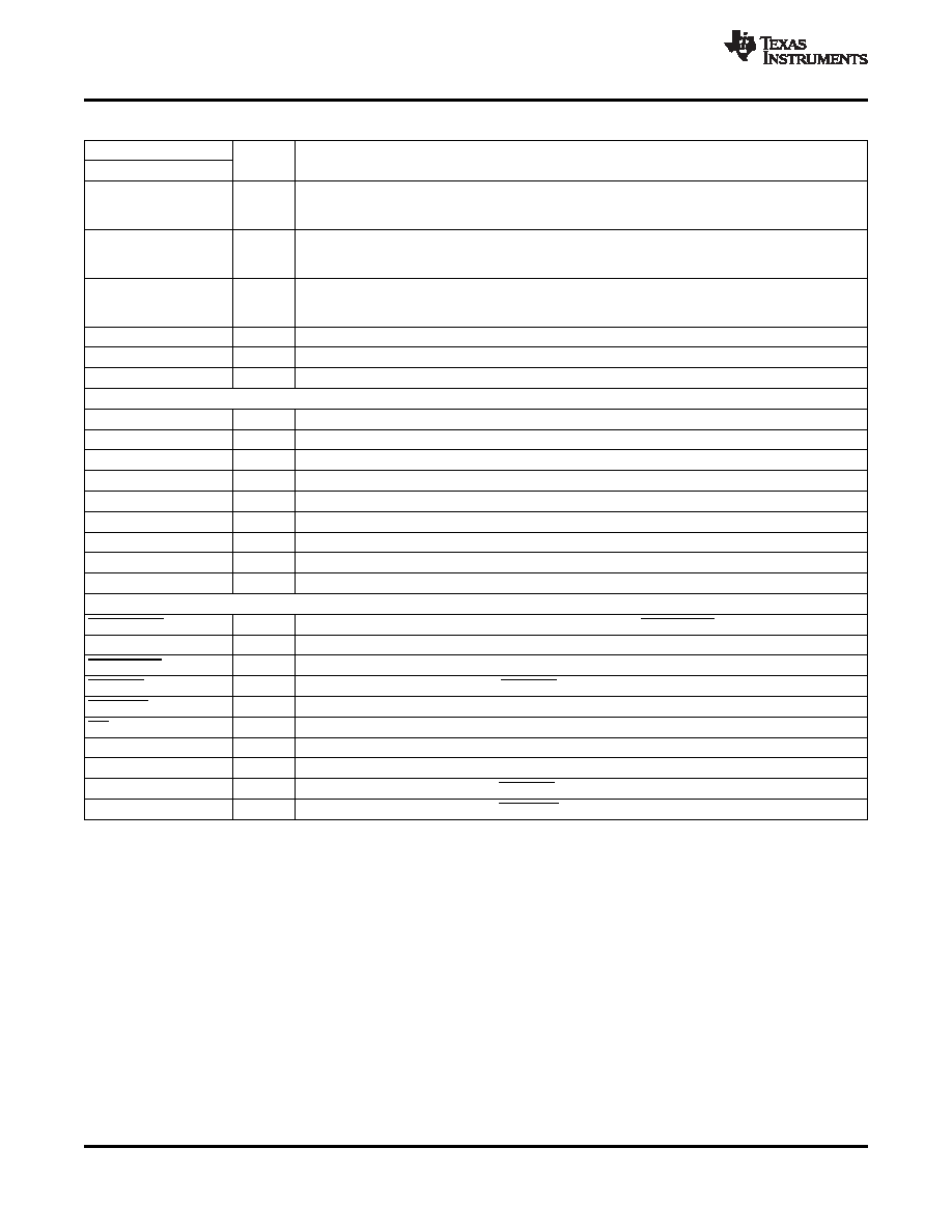
TERMINAL FUNCTIONS (continued)
TERMINAL
I/O
DESCRIPTION
NAME
NO.
Input signal indicating default VDCDC1 voltage, 0 = 1.2 V, 1 = 1.6 V DEFDCDC1 can also be
DEFDCDC1
10
I
connected to a resistor divider between VDCDC1 and GND, if the output voltage of the DCDC1
converter is set in a range from 0.6 V to VINDCDC1 V.
Input signal indicating default VDCDC2 voltage, 0 = 1.8 V, 1 = 3.3 V DEFDCDC2 can also be
DEFDCDC2
32
I
connected to a resistor divider between VDCDC2 and GND, if the output voltage of the DCDC2
converter is set in a range from 0.6 V to VINDCDC2 V.
Input signal indicating default VDCDC3 voltage, 0 = 1.8 V, 1 = 3.3 V DEFDCDC3 can also be
DEFDCDC3
1
I
connected to a resistor divider between VDCDC3 and GND, if the output voltage of the DCDC3
converter is set in a range from 0.6 V to VINDCDC3 V.
DCDC1_EN
25
I
VDCDC1 enable pin. A logic high enables the regulator, a logic low disables the regulator.
DCDC2_EN
24
I
VDCDC2 enable pin. A logic high enables the regulator, a logic low disables the regulator.
DCDC3_EN
23
I
VDCDC3 enable pin. A logic high enables the regulator, a logic low disables the regulator.
LDO REGULATOR SECTION
VINLDO
19
I
Input voltage for LDO1 and LDO2
VLDO1
20
O
Output voltage of LDO1
VLDO2
18
O
Output voltage of LDO2
LDO_EN
22
I
Enable input for LDO1 and LDO2. A Logic high enables the LDOs, a logic low disables the LDOs.
VBACKUP
15
I
Connect the backup battery to this input pin.
VRTC
16
O
Output voltage of the LDO/switch for the real time clock.
VSYSIN
14
I
Input of system voltage for VRTC switch.
DEFLD01
12
I
Digital input. DEFLD01 sets the default output voltage of LDO1 and LDO2.
DEFLD02
13
I
Digital input. DEFLD02 sets the default output voltage of LDO1 and LDO2.
CONTROL AND I2C SECTION
HOT_RESET
11
I
Push button input that reboots or wakes up the processor via RESPWRON output pin.
TRESPWRON
26
I
Connect the timing capacitor to TRESPWRON to set the reset delay time: 1 nF
→ 100 ms.
RESPWRON
27
O
Open drain system reset output.
PWRFAIL
31
O
Open drain output. Active low when PWRFAIL comparator indicates low VBAT condition.
LOW_BAT
21
O
Open drain output of LOW_BAT comparator.
INT
28
O
Open drain output
SCLK
30
I
Serial interface clock line
SDAT
29
I/O
Serial interface data/address
PWRFAIL_SNS
38
I
Input for the comparator driving the PWRFAIL output.
LOWBAT_SNS
39
I
Input for the comparator driving the LOW_BAT output.
12
Copyright 2009–2010, Texas Instruments Incorporated
Product Folder Link(s): TPS65023-Q1
相关PDF资料 |
PDF描述 |
|---|---|
| TS5A3167DBVR | 1-CHANNEL, SGL POLE SGL THROW SWITCH, PDSO5 |
| TPS2375PWR-1 | 1-CHANNEL POWER SUPPLY SUPPORT CKT, PDSO8 |
| TC52N2444ECTTR | 2-CHANNEL POWER SUPPLY SUPPORT CKT, PDSO5 |
| TC52N2532ECTTR | 2-CHANNEL POWER SUPPLY SUPPORT CKT, PDSO5 |
| TC52N2544ECTTR | 2-CHANNEL POWER SUPPLY SUPPORT CKT, PDSO5 |
相关代理商/技术参数 |
参数描述 |
|---|---|
| TPS65023RSBG4 | 制造商:Texas Instruments 功能描述: |
| TPS65023RSBR | 功能描述:电池管理 6Ch Pwr Mgmt IC RoHS:否 制造商:Texas Instruments 电池类型:Li-Ion 输出电压:5 V 输出电流:4.5 A 工作电源电压:3.9 V to 17 V 最大工作温度:+ 85 C 最小工作温度:- 40 C 封装 / 箱体:VQFN-24 封装:Reel |
| TPS65023RSBRG4 | 功能描述:电池管理 6Ch Pwr Mgmt IC RoHS:否 制造商:Texas Instruments 电池类型:Li-Ion 输出电压:5 V 输出电流:4.5 A 工作电源电压:3.9 V to 17 V 最大工作温度:+ 85 C 最小工作温度:- 40 C 封装 / 箱体:VQFN-24 封装:Reel |
| TPS65023RSBT | 功能描述:电池管理 6-Channel Power Management IC RoHS:否 制造商:Texas Instruments 电池类型:Li-Ion 输出电压:5 V 输出电流:4.5 A 工作电源电压:3.9 V to 17 V 最大工作温度:+ 85 C 最小工作温度:- 40 C 封装 / 箱体:VQFN-24 封装:Reel |
| TPS65023RSBT | 制造商:Texas Instruments 功能描述:Power Management IC |
发布紧急采购,3分钟左右您将得到回复。