- 您现在的位置:买卖IC网 > PDF目录69522 > TPS65140PWPR (TEXAS INSTRUMENTS INC) 2.6 A SWITCHING REGULATOR, 2100 kHz SWITCHING FREQ-MAX, PDSO24 PDF资料下载
参数资料
| 型号: | TPS65140PWPR |
| 厂商: | TEXAS INSTRUMENTS INC |
| 元件分类: | 稳压器 |
| 英文描述: | 2.6 A SWITCHING REGULATOR, 2100 kHz SWITCHING FREQ-MAX, PDSO24 |
| 封装: | GREEN, PLASTIC, HTSSOP-24 |
| 文件页数: | 28/31页 |
| 文件大小: | 1391K |
| 代理商: | TPS65140PWPR |
第1页第2页第3页第4页第5页第6页第7页第8页第9页第10页第11页第12页第13页第14页第15页第16页第17页第18页第19页第20页第21页第22页第23页第24页第25页第26页第27页当前第28页第29页第30页第31页
www.ti.com
SLVS497C – SEPTEMBER 2003 – REVISED APRIL 2006
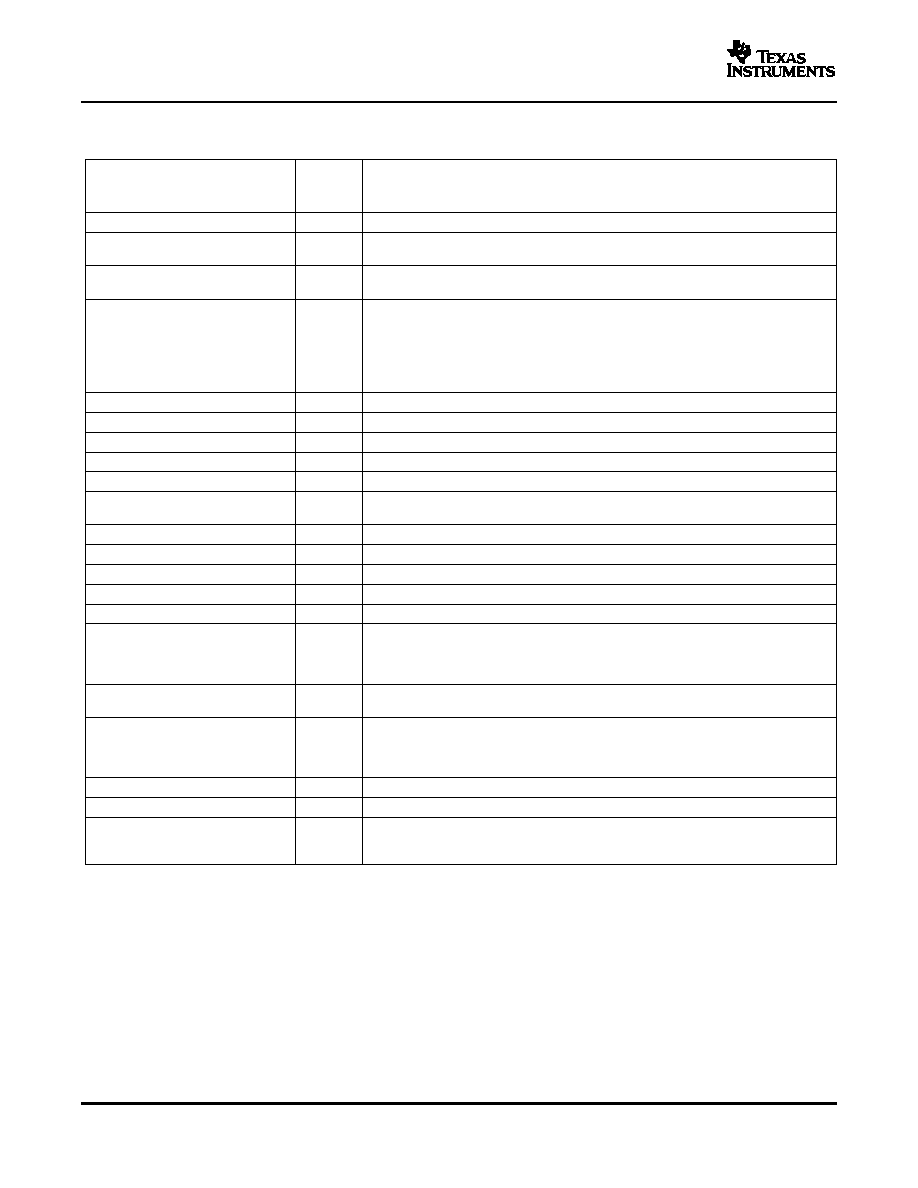
DEVICE INFORMATION (continued)
Terminal Functions
TERMINAL
I/O
DESCRIPTION
NO.
NAME
(PWP)
(RGE)
VIN
4
7
I
Input voltage pin of the device.
Enable pin of the device. This pin should be terminated and not be left floating. A logic
EN
24
3
I
high enables the device and a logic low shuts down the device.
COMP
22
1
Compensation pin for the main boost converter. A small capacitor is connected to this
pin.
Open drain output indicating when all outputs VO1, VO2, VO3 are within 10% of their
PG
10
13
O
nominal output voltage. The output goes low when one of the outputs falls below 10%
of their nominal output voltage.
Enable pin of the linear regulator controller. This pin should be terminated and not be
ENR
23
2
I
left floating. Logic high enables the regulator and a logic low puts the regulator in
shutdown.
C1+
16
19
Positive terminal of the charge pump flying capacitor
C1-
17
20
Negative terminal of the charge pump flying capacitor
DRV
18
21
O
External charge pump driver
FB2
21
24
I
Feedback pin of negative charge pump
REF
20
23
O
Internal reference output typically 1.23 V
Feedback pin of the linear regulator controller. The linear regulator controller is set to a
FB4
2
5
I
fixed output voltage of 3.3 V or 3 V depending on the version.
BASE
3
6
O
Base drive output for the external transistor
GND
11, 19
14, 22
Ground
PGND
7, 8
10, 11
Power ground
FB3
12
15
I
Feedback pin of positive charge pump
OUT3
13
16
O
Positive charge pump output
Negative terminal of the charge pump flying capacitor and charge pump MODE pin. If
the flying capacitor is connected to this pin, the converter operates in a voltage tripler
C2-/MODE
15
18
mode. If the charge pump needs to operate in a voltage doubler mode, the flying
capacitor is removed and the C2-/MODE pin needs to be connected to GND.
Positive terminal for the charge pump flying capacitor. If the device runs in voltage
C2+
14
17
doubler mode, this pin needs to be left open.
Supply pin of the positive, negative charge pump, boost converter, and gate drive
circuit. This pin needs to be connected to the output of the main boost converter and
SUP
9
12
I
cannot be connected to any other voltage source. For performance reasons, it is not
recommended for a bypass capacitor to be connected directly to this pin.
FB1
1
4
I
Feedback pin of the boost converter
SW
5, 6
8, 9
I
Switch pin of the boost converter
PowerPAD
The PowerPAD or exposed thermal die needs to be connected to power ground pins
/Thermal
(PGND)
Die
6
相关PDF资料 |
PDF描述 |
|---|---|
| TPS65140PWPG4 | 2.6 A SWITCHING REGULATOR, 2100 kHz SWITCHING FREQ-MAX, PDSO24 |
| TPS65160PWPG4 | 4.2 A SWITCHING REGULATOR, 900 kHz SWITCHING FREQ-MAX, PDSO28 |
| TPS65160PWPR | 4.2 A SWITCHING REGULATOR, 900 kHz SWITCHING FREQ-MAX, PDSO28 |
| TPS65163RGZR | 4.2 A SWITCHING REGULATOR, 900 kHz SWITCHING FREQ-MAX, PQCC48 |
| TPS65185RGZR | 1-CHANNEL POWER SUPPLY SUPPORT CKT, PQCC48 |
相关代理商/技术参数 |
参数描述 |
|---|---|
| TPS65140PWPRG4 | 功能描述:LCD 驱动器 Trp-Ch 2.1-A Swit Boost Converter RoHS:否 制造商:Maxim Integrated 数位数量:4.5 片段数量:30 最大时钟频率:19 KHz 工作电源电压:3 V to 3.6 V 最大工作温度:+ 85 C 最小工作温度:- 20 C 封装 / 箱体:PDIP-40 封装:Tube |
| TPS65140RGER | 功能描述:LCD 驱动器 Trp-Ch 2.1-A Swit Boost Converter RoHS:否 制造商:Maxim Integrated 数位数量:4.5 片段数量:30 最大时钟频率:19 KHz 工作电源电压:3 V to 3.6 V 最大工作温度:+ 85 C 最小工作温度:- 20 C 封装 / 箱体:PDIP-40 封装:Tube |
| TPS65140RGERG4 | 功能描述:LCD 驱动器 Trp-Ch 2.1-A Swit Boost Converter RoHS:否 制造商:Maxim Integrated 数位数量:4.5 片段数量:30 最大时钟频率:19 KHz 工作电源电压:3 V to 3.6 V 最大工作温度:+ 85 C 最小工作温度:- 20 C 封装 / 箱体:PDIP-40 封装:Tube |
| TPS65141PWP | 功能描述:LCD 驱动器 5V/1.6A(I/O) 4-CH Multi-Converter RoHS:否 制造商:Maxim Integrated 数位数量:4.5 片段数量:30 最大时钟频率:19 KHz 工作电源电压:3 V to 3.6 V 最大工作温度:+ 85 C 最小工作温度:- 20 C 封装 / 箱体:PDIP-40 封装:Tube |
| TPS65141PWPG4 | 功能描述:LCD 驱动器 5V/1.6A(I/O) 4-CH Multi-Converter RoHS:否 制造商:Maxim Integrated 数位数量:4.5 片段数量:30 最大时钟频率:19 KHz 工作电源电压:3 V to 3.6 V 最大工作温度:+ 85 C 最小工作温度:- 20 C 封装 / 箱体:PDIP-40 封装:Tube |
发布紧急采购,3分钟左右您将得到回复。