- 您现在的位置:买卖IC网 > PDF目录69523 > TPS84410RKGR (TEXAS INSTRUMENTS INC) 4 A SWITCHING REGULATOR, 600 kHz SWITCHING FREQ-MAX, PQCC39 PDF资料下载
参数资料
| 型号: | TPS84410RKGR |
| 厂商: | TEXAS INSTRUMENTS INC |
| 元件分类: | 稳压器 |
| 英文描述: | 4 A SWITCHING REGULATOR, 600 kHz SWITCHING FREQ-MAX, PQCC39 |
| 封装: | 9 X 11 MM, 2.80 MM HEIGHT, GREEN, PLASTIC, BQFN-39 |
| 文件页数: | 23/26页 |
| 文件大小: | 819K |
| 代理商: | TPS84410RKGR |
SLVSAR5
– SEPTEMBER 2011
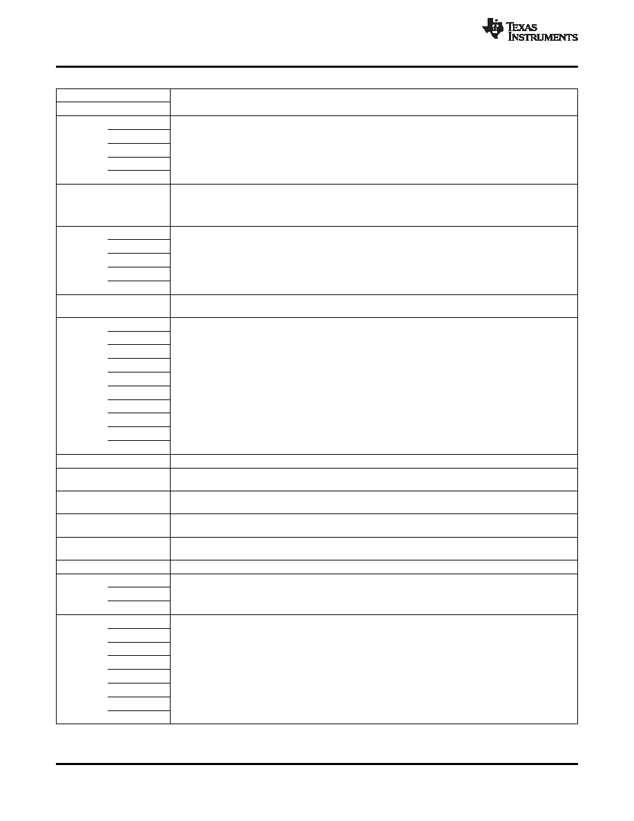
PIN DESCRIPTIONS
TERMINAL
DESCRIPTION
NAME
NO.
1
Zero VDC reference for the analog control circuitry. These pins should be connected directly to the PCB
5
analog ground plane. Not all pins are connected together internally. All pins must be connected together
AGND
29
externally with a copper plane or pour directly under the module. Connect the AGND copper area to the
PGND copper area at a single point; directly at the pin 37 PowerPAD using multiple vias. See the
33
recommended layout in Figure 34.
34
This pad provides both an electrical and thermal connection to the PCB. This pad should be connected
PowerPAD
directly to the PCB power ground plane using multiple vias for good electrical and thermal performance. The
37
(PGND)
same vias should also be used to connect to the PCB analog ground plane. See the recommended layout in
2
3
Do not connect. Do not connect these pins to AGND, to another DNC pin, or to any other voltage. These
DNC
15
pins are connected to internal circuitry. Each pin must be soldered to an isolated pad.
16
26
Inhibit and UVLO adjust pin. Use an open drain or open collector output logic to control the INH function. A
INH/UVLO
28
resistor between this pin and AGND adjusts the UVLO voltage.
17
18
19
20
21
Phase switch node. These pins should be connected by a small copper island under the device for thermal
PH
relief. Do not connect any external component to this pin or tie it to a pin of another function.
22
23
24
25
39
PWRGD
27
Power good fault pin. Asserts low if the output voltage is out of tolerance. A pull-up resistor is required.
This pin automatically selects between RT mode and CLK mode. An external timing resistor adjusts the
RT/CLK
4
switching frequency of the device. In CLK mode, the device synchronizes to an external clock.
Remote sense connection. Connect this pin to VOUT at the load for improved regulation. This pin must be
SENSE+
36
connected to VOUT at the load, or at the module pins.
Slow-start and tracking pin. Connecting an external capacitor to this pin adjusts the output voltage rise time.
SS/TR
6
A voltage applied to this pin allows for tracking and sequencing control.
Slow-start or track feature select. Connect this pin to AGND to enable the internal SS capacitor with a SS
STSEL
7
interval of approximately 1.1 ms. Leave this pin open to enable the TR feature.
VADJ
35
Connecting a resistor between this pin and AGND sets the output voltage above the 0.8V default voltage.
30
The positive input voltage power pins, which are referenced to PGND. Connect external input capacitance
VIN
31
between these pins and the PGND plane, close to the device.
32
8
9
10
11
VOUT
Output voltage. Connect output capacitors between these pins and the PGND plane, close to the device.
12
13
14
38
6
Copyright
2011, Texas Instruments Incorporated
相关PDF资料 |
PDF描述 |
|---|---|
| TQN25A48S12 | 1-OUTPUT 300 W DC-DC REG PWR SUPPLY MODULE |
| TQN25A48S12 | 1-OUTPUT 300 W DC-DC REG PWR SUPPLY MODULE |
| TQN20A48S12 | 1-OUTPUT 240 W DC-DC REG PWR SUPPLY MODULE |
| TRF2020PW | PLL FREQUENCY SYNTHESIZER, 1200 MHz, PDSO24 |
| TRF2040PWLE | PLL FREQUENCY SYNTHESIZER, 2200 MHz, PDSO24 |
相关代理商/技术参数 |
参数描述 |
|---|---|
| TPS84410RKGT | 功能描述:直流/直流开关转换器 3V-6Vin,4A Sync Buck Int Pwr Sol RoHS:否 制造商:STMicroelectronics 最大输入电压:4.5 V 开关频率:1.5 MHz 输出电压:4.6 V 输出电流:250 mA 输出端数量:2 最大工作温度:+ 85 C 安装风格:SMD/SMT |
| TPS844F | 制造商:TOSHIBA 制造商全称:Toshiba Semiconductor 功能描述:Silicon Epitaxial Planar |
| TPS84610 | 制造商:TI 制造商全称:Texas Instruments 功能描述:2.95-V to 6-V Input, 6-A Synchronous Buck, Integrated Power Solution |
| TPS84610EVM-003 | 功能描述:电源管理IC开发工具 TPS84610 Eval Mod RoHS:否 制造商:Maxim Integrated 产品:Evaluation Kits 类型:Battery Management 工具用于评估:MAX17710GB 输入电压: 输出电压:1.8 V |
| TPS84610RKG | 制造商:TI 制造商全称:Texas Instruments 功能描述:2-A to 6-A Integrated Power Solution |
发布紧急采购,3分钟左右您将得到回复。