- 您现在的位置:买卖IC网 > PDF目录150822 > TRU050GBLGA49.152 (VECTRON INTERNATIONAL) PHASE LOCKED LOOP, CDSO16 PDF资料下载
参数资料
| 型号: | TRU050GBLGA49.152 |
| 厂商: | VECTRON INTERNATIONAL |
| 元件分类: | PLL合成/DDS/VCOs |
| 英文描述: | PHASE LOCKED LOOP, CDSO16 |
| 封装: | ROHS COMPLIANT, HERMETIC SEALED, CERAMIC, SMD, DIP-16 |
| 文件页数: | 9/14页 |
| 文件大小: | 0K |
| 代理商: | TRU050GBLGA49.152 |
TRU050, VCXO Based PLL
Vectron International, 267 Lowell Rd, Hudson NH 03051-4916
Tel: 1-88-VECTRON-1
Web: www.vectron.com
Page 4 of 14
Rev : 06Jan2006
TRU050 Theory of Operation
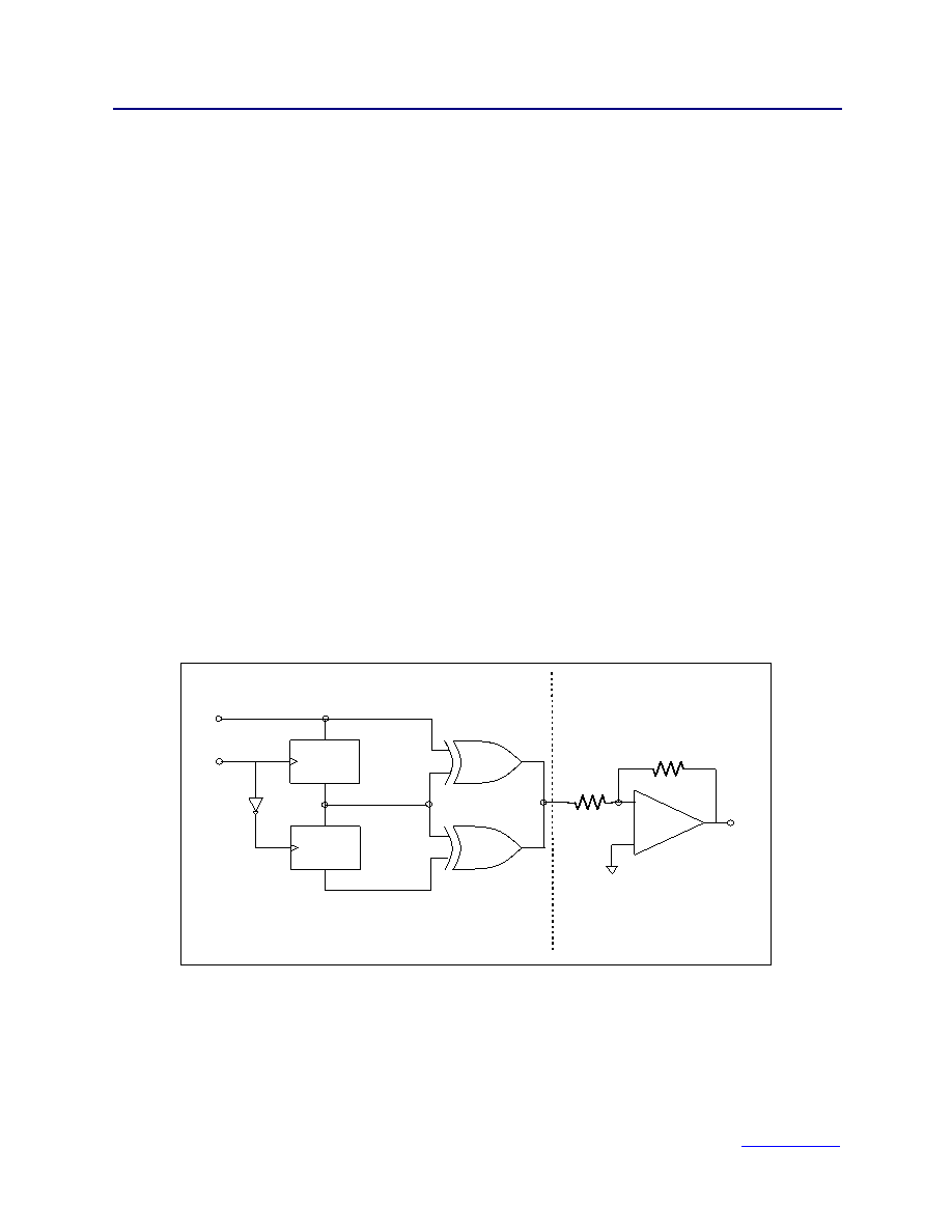
Phase Detector
The phase detector has two buffered inputs, DATAIN and CLKIN, which are designed to switch at 1.4
volts. DATAIN is designed to accept an NRZ data stream but may also be used for clock signals which
have about a 50% duty cycle. CLKIN is connected to OUT1 or OUT2, or a divided version of one of these
outputs. CLKIN and DATAIN and are protected by ESD diodes and should not exceed the power supply
voltage or ground by more than a few hundred millivolts.
The phase detector is basically a latched flip flop/exclusive-or gate/differential amplifier filter design to
produce a DC signal proportional to the phase between the CLKIN and DATAIN signals, see figure 4 for a
block diagram and figure 5 for a open loop transfer curve. This simplies the PLL design as the designer
does not have to filter narrow pulse signal to a DC level. Under locked conditions the rising edge CLKIN
will be centered in the middle of the DATAIN signal, see figure 6.
The phase detector gain is 0.53V/rad x data density for 5volt operation, and 0.35V/rad x data density for
3.3 volt operation. Data density = 1.0 for clock signals and is system dependent on coding and design
for NRZ signals, but 0.25 could be used as a starting point for data density.
The phase detector output is a DC signal for DATAIN frequencies greater than 1MHz but produces
signficant ripple when inputs are less than 200kHz. Additional filtering is required for low input frequency
applications such as 8kHz frequency translation, see figures 8 and 9.
Under closed loop conditions the active filter has a blocking capacitor which provides a very high DC
gain, so under normal locked conditions and input frequencies >1MHz, PHO will be about VDD/2 and will
not vary signifigantly with changes in input frequency (within lock range). The control (voltage pin 1) will
vary according to the input frequency offset, but PHO will remain relatively constant.
D
Q1
Q2
D
Gain = 2 / 3
Gain = 5 V / 2
π
30 k
20 k
PHO
(pin 6)
Clock In
(pin 9)
Data In
(pin 7)
Figure 4. Simplified Phase Detector Block Diagram
相关PDF资料 |
PDF描述 |
|---|---|
| TRU050GBLHA16.128 | PHASE LOCKED LOOP, CDSO16 |
| TRU050GCCGA25.248 | PHASE LOCKED LOOP, CDSO16 |
| TRU050GCCHB33.33 | PHASE LOCKED LOOP, CDSO16 |
| TRU050GCCNB16.384 | PHASE LOCKED LOOP, CDSO16 |
| TRU050GCLGB17.92 | PHASE LOCKED LOOP, CDSO16 |
相关代理商/技术参数 |
参数描述 |
|---|---|
| TRU050-GBLGA-65M0000000 | 制造商:VECTRON 制造商全称:Vectron International, Inc 功能描述:Complete VCXO based Phase-Locked Loop |
| TRU050-GBLGB-1M0000000 | 制造商:VECTRON 制造商全称:Vectron International, Inc 功能描述:Complete VCXO based Phase-Locked Loop |
| TRU050-GBLGB-65M0000000 | 制造商:VECTRON 制造商全称:Vectron International, Inc 功能描述:Complete VCXO based Phase-Locked Loop |
| TRU050-GBLHA | 制造商:未知厂家 制造商全称:未知厂家 功能描述:SINGLE DROP IN QUARTZ STABILIZED PLL SOLUTUION |
| TRU050-GBLHA-1M0000000 | 制造商:VECTRON 制造商全称:Vectron International, Inc 功能描述:Complete VCXO based Phase-Locked Loop |
发布紧急采购,3分钟左右您将得到回复。