- 您现在的位置:买卖IC网 > PDF目录272821 > TS12A4516D (TEXAS INSTRUMENTS INC) 1-CHANNEL, SGL POLE SGL THROW SWITCH, PDSO8 PDF资料下载
参数资料
| 型号: | TS12A4516D |
| 厂商: | TEXAS INSTRUMENTS INC |
| 元件分类: | 多路复用及模拟开关 |
| 英文描述: | 1-CHANNEL, SGL POLE SGL THROW SWITCH, PDSO8 |
| 封装: | GREEN, PLASTIC, SOIC-8 |
| 文件页数: | 14/16页 |
| 文件大小: | 619K |
| 代理商: | TS12A4516D |
APPLICATION INFORMATION
Power-Supply Considerations
Logic-Level Thresholds
Test Circuits/Timing Diagrams
NO
orNC
www.ti.com ................................................................................................................................................. SCDS236B – DECEMBER 2006 – REVISED APRIL 2009
The TS12A4516 and TS12A4517 operate with power-supply voltages from ±1 V to ±6 V [(2 V < (V+ – V–) < 12 V],
but are tested and specified at ±5V, ±3.3V, and ±1.8V supplies. The pin-compatible TS12A4514 and TS12A4515
are recommended for use when only a single supply is desirable.
The TS12A4516 and TS12A4517 construction is typical of most CMOS analog switches, except that they have
only two supply pins: V+ and V–. V+ and V– drive the internal CMOS switches and set their analog voltage limits.
Reverse ESD-protection diodes are internally connected between each analog-signal pin and both V+ and V–.
One of these diodes conducts if any analog signal exceeds V+ or V–.
Virtually all the analog leakage current comes from the ESD diodes to V+ or V–. Although the ESD diodes on a
given signal pin are identical and, therefore, fairly well balanced, they are reverse biased differently. Each is
biased by either V+ or V– and the analog signal. This means their leakages will vary as the signal varies. The
difference in the two diode leakages to the V+ and V– pins constitutes the analog-signal-path leakage current. All
analog leakage current flows between each pin and one of the supply terminals, not to the other switch terminal.
This is why both sides of a given switch can show leakage currents of the same or opposite polarity.
V+ and V– also power the internal logic and logic-level translators. The logic-level translators convert the logic
levels to switched V+ and V– signals to drive the analog signal gates.
Since these parts have no ground pin, the logic-level threshold is referenced to V+. The threshold limits are V+
–1.5 V and V+ –3.5 V for V+ levels between 6 V and 3 V. When V+ = 2 V, the logic threshold is approximately 0.6
V.
CAUTION:
Do not connect the TS12A4516/TS12A4517 V+ to 3 V and then connect the
logic-level pins to logic-level signals that operate from 5-V supply. TTL levels
can exceed 3 V and violate the absolute maximum ratings, damaging the part
and/or external circuits.
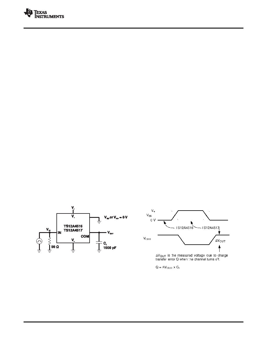
Figure 1. Charge Injection
Copyright 2006–2009, Texas Instruments Incorporated
7
相关PDF资料 |
PDF描述 |
|---|---|
| TL7705BIDRG4 | 1-CHANNEL POWER SUPPLY SUPPORT CKT, PDSO8 |
| TL7660CDGKR | SWITCHED CAPACITOR CONVERTER, 9 kHz SWITCHING FREQ-MAX, PDSO8 |
| TL7660ID | SWITCHED CAPACITOR CONVERTER, 9 kHz SWITCHING FREQ-MAX, PDSO8 |
| TPS65562RGTT | 3 A BATTERY CHARGE CONTROLLER, PQCC16 |
| TL431LP | 1-OUTPUT THREE TERM VOLTAGE REFERENCE, BCY3 |
相关代理商/技术参数 |
参数描述 |
|---|---|
| TS12A4516DBVR | 功能描述:模拟开关 IC Lo-Vltg,Lo On-St Res SPST CMOS Ana Sw RoHS:否 制造商:Texas Instruments 开关数量:2 开关配置:SPDT 开启电阻(最大值):0.1 Ohms 切换电压(最大): 开启时间(最大值): 关闭时间(最大值): 工作电源电压:2.7 V to 4.5 V 最大工作温度:+ 85 C 安装风格:SMD/SMT 封装 / 箱体:DSBGA-16 |
| TS12A4516DG4 | 功能描述:模拟开关 IC Lo-Vltg Lo On-St Resist SPST CMOS RoHS:否 制造商:Texas Instruments 开关数量:2 开关配置:SPDT 开启电阻(最大值):0.1 Ohms 切换电压(最大): 开启时间(最大值): 关闭时间(最大值): 工作电源电压:2.7 V to 4.5 V 最大工作温度:+ 85 C 安装风格:SMD/SMT 封装 / 箱体:DSBGA-16 |
| TS12A4516DR | 功能描述:模拟开关 IC Lo-Vltg Lo On-St Resist SPST CMOS RoHS:否 制造商:Texas Instruments 开关数量:2 开关配置:SPDT 开启电阻(最大值):0.1 Ohms 切换电压(最大): 开启时间(最大值): 关闭时间(最大值): 工作电源电压:2.7 V to 4.5 V 最大工作温度:+ 85 C 安装风格:SMD/SMT 封装 / 箱体:DSBGA-16 |
| TS12A4516DRG4 | 功能描述:模拟开关 IC Lo-Vltg Lo On-St Resist SPST CMOS RoHS:否 制造商:Texas Instruments 开关数量:2 开关配置:SPDT 开启电阻(最大值):0.1 Ohms 切换电压(最大): 开启时间(最大值): 关闭时间(最大值): 工作电源电压:2.7 V to 4.5 V 最大工作温度:+ 85 C 安装风格:SMD/SMT 封装 / 箱体:DSBGA-16 |
| TS12A4516P | 制造商:TI 制造商全称:Texas Instruments 功能描述:DUAL SUPPLY, LOW ON-STATE RESISTANCE SPST CMOS ANALOG SWITCHES |
发布紧急采购,3分钟左右您将得到回复。