- 您现在的位置:买卖IC网 > PDF目录97319 > TS2043G-R16-R (UNISONIC TECHNOLOGIES CO LTD) 4-CH 12-BIT SUCCESSIVE APPROXIMATION ADC, SERIAL ACCESS, PDSO16 PDF资料下载
参数资料
| 型号: | TS2043G-R16-R |
| 厂商: | UNISONIC TECHNOLOGIES CO LTD |
| 元件分类: | ADC |
| 英文描述: | 4-CH 12-BIT SUCCESSIVE APPROXIMATION ADC, SERIAL ACCESS, PDSO16 |
| 封装: | 0.150 INCH, HALOGEN FREE, SSOP-16 |
| 文件页数: | 7/8页 |
| 文件大小: | 203K |
| 代理商: | TS2043G-R16-R |
TS2043
Preliminary
CMOS IC
UNISONICTECHNOLOGIESCO.,LTD
7 of 8
www.unisonic.com.tw
QW-R502-404.a
APPLICATION INFORMATION(Cont.)
Serial Interface
Once a falling signal applies on /CS pin (active in low), the operation is initiated. After /CS falls, the UTC
TS2043
begins to look for a start bit on the DIN input. At the end of the operation the /CS pin should be pulled high,
which minimizes supply current if DCLK is left running.
Control Byte
The first eight clock cycles provides the control byte on DIN pin. (See Table I and Table II for more information).
The control byte represents the start operation, addressing, resolution, and power down information.
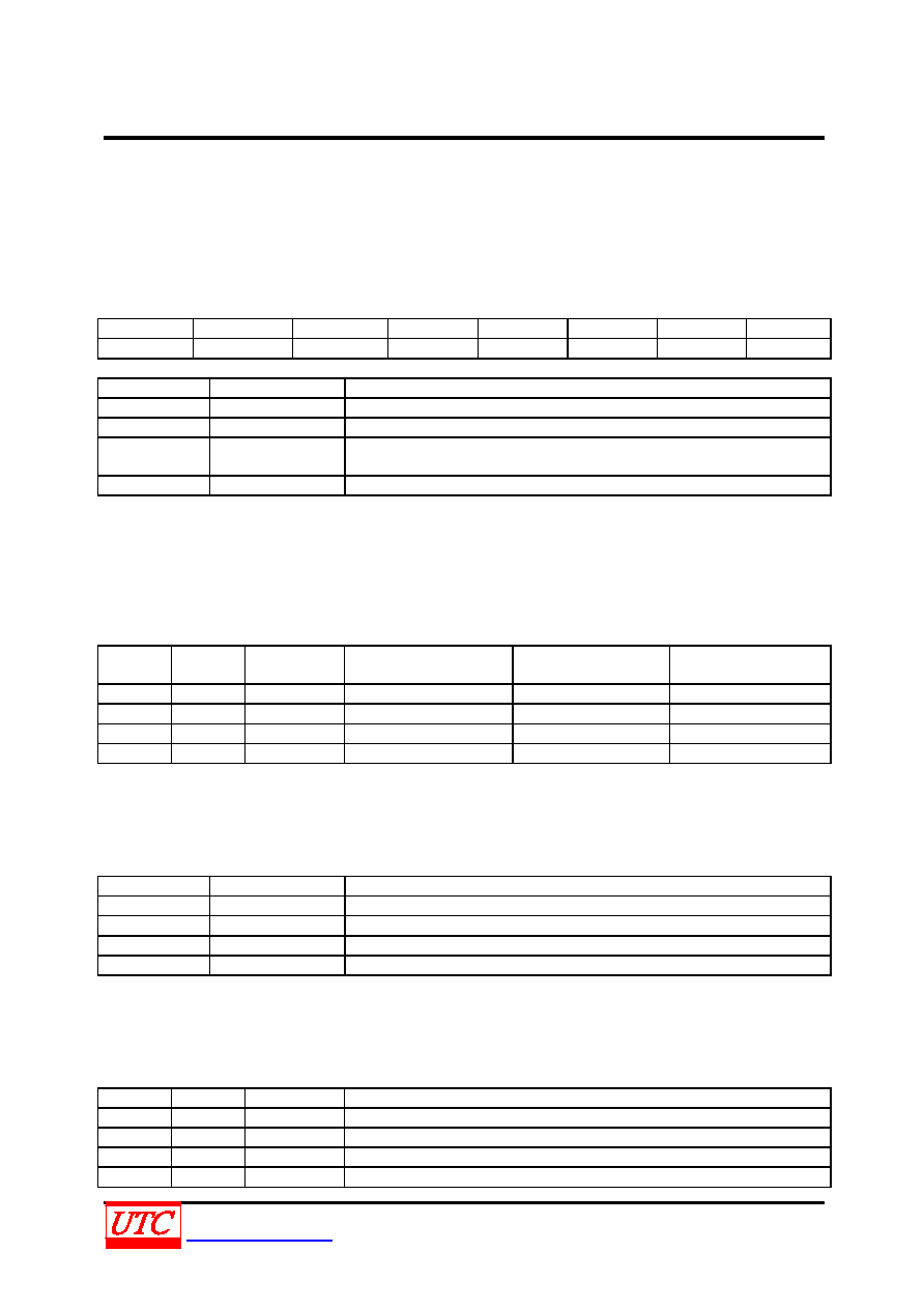
Table I. Control Bits in the Control Byte
Bit 7
Bit 6
Bit 5
Bit 4
Bit 3
Bit 2
Bit 1
Bit 0
Start
A2
A1
A0
Mode1
Mode0
PD1
PD0
Table II. Description of the Control Bits
BIT
NAME
DESCRIPTION
7
Start
Start Bit.
6,5,4
A2,A1,A0
Input Channel Select Bits.
3,2
Mode1
Mode0
12-Bit / 8-Bit Conversion
Configuration Bit.
1,0
PD1,PD0
Power Down Control Bits
Start Bit – Initiate Start
The control byte starts with the first high bit on DIN. The first bit must always be logic high (1) to initiate the start
of the conversion. The UTC TS2043 will not start until the start bit is detected.
Addressing Bits – Input Channel Selection
The next three bits on control byte are addressing bits (A2, A1, A0), which select the active input channel of the
input multiplexer, and touch panel drivers. (See Table III for more information).
Table III. Input Channel Configuration
A2
A1
Input
Channel
X Switch
Y Switch
Reference
0
X+
OFF
ON
VREF
1
0
Y+
ON
OFF
VREF
0
1
IN3
OFF
VREF
1
IN4
OFF
VREF
Mode Bits – Conversion Resolution Configuration
The Mode bits (Mode1, Mode0) set the resolution of this device. With the Mode1 bit LOW (0), the following
conversion will have 12 bits of resolution. With the Mode1 bit HIGH (1) the following conversion will have 8 bits of
resolution. (See Table IV for more information.)
Table IV. Resolution Configuration
Mode1
Mode0
DESCRIPTION
0
1
12bits Resolution
0
12bits Resolution
1
8bits Resolution
1
0
8bits Resolution
PD0 and PD1 Bits - Power Down Control
The last two bits are PD1 and PD0 bits, which control the power down mode of the UTC TS2043. Through
applying a same logic high(1) this device enters a power-up mode, while enters a power-down mode by a same
logic low (0) on PD1 and PD0 bits.(See Table V for more information).
Table V. Power-Down Selection
PD1
PD0
PENIRQ
DESCRIPTION
0
Enable
Power-Down between conversions. Y- switch is on.
0
1
Disable
Power-Down between conversions. Y- switch is off. /PENIRQ is disabled
1
0
Disable
No used.
1
Disable
No Power-Down between conversions.
相关PDF资料 |
PDF描述 |
|---|---|
| TS2496CM33RN | SWITCHING REGULATOR, 173 kHz SWITCHING FREQ-MAX, PSSO5 |
| TS2496CM50RN | SWITCHING REGULATOR, 173 kHz SWITCHING FREQ-MAX, PSSO5 |
| TS2508ACSRL | 3 A SWITCHING REGULATOR, 400 kHz SWITCHING FREQ-MAX, PDSO8 |
| TS3-D0A31 | 1 FUNCTIONS, 130.05 MHz, 14 kHz BW(delta f), MONOLITHIC CRYSTAL FILTER |
| TF3-J3DC5 | 1 FUNCTIONS, 183.6 MHz, 13 kHz BW(delta f), MONOLITHIC CRYSTAL FILTER |
相关代理商/技术参数 |
参数描述 |
|---|---|
| TS204R | 制造商:TRSYS 制造商全称:Transys Electronics 功能描述:FAST SWITCHIING RECTIFIER(Reverse Voltage - 50 to 1000 Volts, Current - 2.0Ampere) |
| TS20521AS | 制造商:Lovato Electric Inc 功能描述: |
| TS2056 | 制造商:Touchstone Technology Inc. 功能描述:8.4" R48.412T - Bulk |
| TS2060IP | 制造商:Enhance Technology 功能描述:ENHANCERAID,ISCSI INTERFAC - Bulk |
| TS2060IS-IP | 制造商:Enhance Technology 功能描述:ENHANCERAID - Bulk |
发布紧急采购,3分钟左右您将得到回复。