- 您现在的位置:买卖IC网 > PDF目录373697 > TS258CD (Taiwan Semiconductor Co., Ltd.) Dual Operating Amplifier PDF资料下载
参数资料
| 型号: | TS258CD |
| 厂商: | Taiwan Semiconductor Co., Ltd. |
| 英文描述: | Dual Operating Amplifier |
| 中文描述: | 双运放 |
| 文件页数: | 2/6页 |
| 文件大小: | 168K |
| 代理商: | TS258CD |
TS258
2-6
2005/02 rev. A
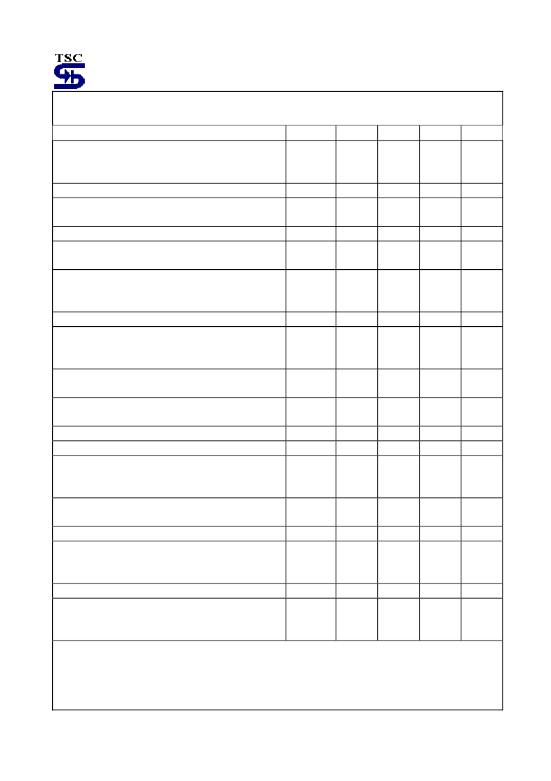
Electrical Characteristics
(V
CC
= 5V, Ta=25
o
C; unless otherwise specified.)
Characteristics
Symbol
Min
Typ
Max
Unit
Input Offset Voltage
V
CC
= 5.0V to 30V, V
IC
= 0V to Vcc -1.7 V, Vo= 1.4V, R
S
= 0
T
LOW
≤
Ta
≤
T
HIGH
Vio
--
--
2.0
--
5.0
7.0
mV
Average Temperature Coefficient of Input Offset Voltage
Iio/
T
△
△
--
7.0
--
uV/
o
C
Input Offset Current
T
LOW
≤
Ta
≤
T
HIGH
Iio
--
--
5.0
--
50
150
nA
Average Temperature Coefficient of input Offset Current
Iio/
T
△
△
--
10
--
pA/
o
C
Input Bias Current
T
LOW
≤
Ta
≤
T
HIGH
Input Common-Mode Voltage Range (Note1)
I
IB
--
45
50
-250
-500
uA
V
CC
= 30 V
V
CC
= 30 V, T
LOW
≤
Ta
≤
T
HIGH
V
ICR
0
0
--
--
28.3
28
V
Differential Input Voltage Range
V
IDR
--
--
V
CC
V
Large Signal Open-Loop Voltage Gain
R
L
= 2.0K, V
CC
=15V, For Large V
O
Swing,
T
LOW
≤
Ta
≤
T
HIGH
A
VOL
25
15
100
--
--
--
V/mV
Channel Separation
1.0 KHz to 20KHz
--
--
-120
--
dB
Common Mode Rejection Ratio
R
S
≤
10 k
CMRR
65
70
--
dB
Power Supply Rejection Ratio
PSRR
65
100
--
dB
Output Voltage Range, RL = 2K
V
OR
0
--
3.3
V
Output Voltage -- High Limit
V
CC
= 30 V, R
L
= 2 k
V
CC
= 30 V, R
L
= 10 k
V
OH
26
27
--
28
--
--
V
Output Voltage -- Low Limit
V
CC
= 5.0 V, R
L
= 10 k
V
OL
--
5.0
20
mV
Output Source Current V
ID
=+1.0V,V
CC
=15V
I
O+
20
40
--
mA
Output Sink Current
V
ID
= -1.0 V, V
CC
= 15 V
V
ID
= -1.0 V, V
O
= 200 mV
I
O-
10
12
20
50
--
--
mA
uA
Output Short Circuit to Ground (Note 2)
I
OS
--
40
60
mA
Power Supply Current ,
V
CC
= 30 VV
O
= 0 V, R
L
=
∞
V
CC
= 5.0 V, V
O
= 0 V, R
L
=
∞
Notes :
1. The input common mode voltage or either input signal voltage should not be allowed to go negative by more than
0.3 V. The upper end of the common mode voltage range is Vcc 17V, but either or both inputs can go to +32V.
2. Short circuits from the output to Vcc can cause excessive heating and eventual destruction. Destructive dissipation
can recruit from simultaneous shorts on all amplifiers.
I
CC
--
--
1.5
0.7
3.0
1.2
mA
相关PDF资料 |
PDF描述 |
|---|---|
| TS258CS | Dual Operating Amplifier |
| TS2596CZ55.0 | 3A Step Down Switching Voltage Regulator |
| TS2596CM5 | 3A Step Down Switching Voltage Regulator |
| TS2596CM505 | 3A Step Down Switching Voltage Regulator |
| TS2596CM53.3 | 3A Step Down Switching Voltage Regulator |
相关代理商/技术参数 |
参数描述 |
|---|---|
| TS258CS | 制造商:TSC 制造商全称:Taiwan Semiconductor Company, Ltd 功能描述:Dual Operating Amplifier |
| TS2596 | 制造商:TSC 制造商全称:Taiwan Semiconductor Company, Ltd 功能描述:3A / 150KHz Buck Dc-Dc Converter |
| TS2596_07 | 制造商:TSC 制造商全称:Taiwan Semiconductor Company, Ltd 功能描述:3A / 150KHz Buck Dc-Dc Converter |
| TS2596_08 | 制造商:TSC 制造商全称:Taiwan Semiconductor Company, Ltd 功能描述:3A / 150KHz Buck Dc-Dc Converter |
| TS2596CM | 制造商:TSC 制造商全称:Taiwan Semiconductor Company, Ltd 功能描述:3A / 150KHz Buck Dc-Dc Converter |
发布紧急采购,3分钟左右您将得到回复。