- 您现在的位置:买卖IC网 > PDF目录373702 > TS339IYDT (意法半导体) Micropower Quad CMOS Voltage Comparators PDF资料下载
参数资料
| 型号: | TS339IYDT |
| 厂商: | 意法半导体 |
| 英文描述: | Micropower Quad CMOS Voltage Comparators |
| 中文描述: | 微四路CMOS电压比较器 |
| 文件页数: | 2/9页 |
| 文件大小: | 117K |
| 代理商: | TS339IYDT |
Absolute Maximum Ratings
TS339
2/9
1
Absolute Maximum Ratings
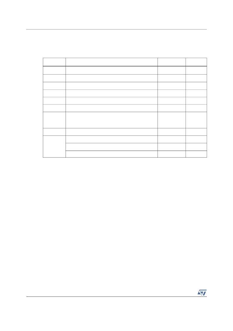
Table 1.
Key parameters and their absolute maximum ratings
Symbol
Parameter
Value
Unit
V
CC+
Supply Voltage
(1)
1.
All voltage values, except differential voltage, are with respect to network ground terminal.
18
V
V
id
Differential Input Voltage
(2)
2.
Differential voltages are the non-inverting input terminal with respect to the inverting input terminal.
±18
V
V
i
Input Voltage
(3)
3.
Excursions of input voltages may exceed the power supply level. As long as the common mode voltage
[V
icm
=(V
in+
+ V
in-
)/2] remains within the specified range, the comparator will provide a stable output state.
However, the maximum current through the ESD diodes (IF) of the input stage must strictly be observed.
18
V
V
o
Output Voltage
18
V
I
o
Output Current
20
mA
I
F
Forward Current in ESD Protection Diodes on Inputs
(4)
4.
Guaranteed by design.
50
mA
p
d
Power Dissipation
(5)
DIP14
SO14
TSSOP14
5.
Pd is calculated with T
amb
= +25°C, T
j
= +150°C and
R
thja
= 80 °C/W for DIP14 package
R
thja
= 150 °C/W for SO14 package
R
thja
= 175°C/W for TSSOP14 package
1500
830
710
mW
T
stg
Storage Temperature Range
-65 to +150
°C
ESD
HBM: Human Body Model
(6)
6.
Human body model, 100pF discharged through a 1.5k
resistor into pin of device.
50
V
MM: Machine Model
(7)
7.
Machine model ESD, a 200pF cap is charged to the specified voltage, then discharged directly into the IC with
no external series resistor (internal resistor < 5
), into pin to pin of device.
40
V
CDM: Charged Device Model
800
V
相关PDF资料 |
PDF描述 |
|---|---|
| TS3404CD | PWM Buck Controller |
| TS3404 | PWM Buck Controller |
| TS3404CS | PWM Buck Controller |
| TS3405 | Single Synchronous Buck PWM Controller |
| TS3405CS | Single Synchronous Buck PWM Controller |
相关代理商/技术参数 |
参数描述 |
|---|---|
| TS339M | 制造商:STMICROELECTRONICS 制造商全称:STMicroelectronics 功能描述:MICROPOWER QUAD CMOS VOLTAGE COMPARATORS |
| TS339MD | 制造商:未知厂家 制造商全称:未知厂家 功能描述:Analog Comparator |
| TS339MJ | 制造商:未知厂家 制造商全称:未知厂家 功能描述:Analog Comparator |
| TS339MN | 制造商:未知厂家 制造商全称:未知厂家 功能描述:VOLT COMPARATOR|QUAD|CMOS|DIP|14PIN|PLASTIC |
| TS339MP | 制造商:未知厂家 制造商全称:未知厂家 功能描述:Analog Comparator |
发布紧急采购,3分钟左右您将得到回复。