- 您现在的位置:买卖IC网 > PDF目录373705 > TS391 (意法半导体) LOWPOWER SINGLE VOLTAGE COMPARATORS PDF资料下载
参数资料
| 型号: | TS391 |
| 厂商: | 意法半导体 |
| 元件分类: | 比较器 |
| 英文描述: | LOWPOWER SINGLE VOLTAGE COMPARATORS |
| 中文描述: | 低功率单电压比较器 |
| 文件页数: | 3/5页 |
| 文件大小: | 44K |
| 代理商: | TS391 |
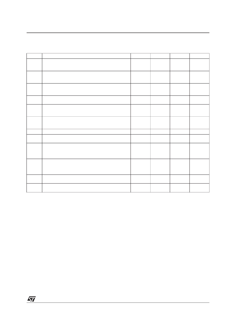
ELECTRICAL CHARACTERISTICS
V
CC+
= +5V, V
CC–
= 0V, T
amb
= 25
o
C (unless otherwise specified)
Symbol
V
io
Parameter
Min.
Typ.
Max.
Unit
mV
Input Offset Voltage – (note 2)
T
amb
= +25
o
C
T
min
.
≤
T
amb
≤
T
max.
Input Bias Current – (note 3)
T
amb
= +25
o
C
T
min
.
≤
T
amb
≤
T
max.
Input Offset Current
T
amb
= +25
o
C
T
min
.
≤
T
amb
≤
T
max.
Large Signal Voltage Gain
V
CC
= 15V, R
L
= 15k
, V
o
= 1 to 11V
Supply Current
V
CC
=
5V, no load
V
CC
= 30V, no load
Input Common Mode Voltage Range - (note 4)
T
amb
= +25
o
C
T
min
.
≤
T
amb
≤
T
max.
Differential Input Voltage - (note 6)
Output Sink Current
(V
id
= -1V, V
O
= 1.5V)
Low Level Output Voltage
(V
id
= -1V, I
sink
= 4mA)
T
amb
= 25
o
C
T
min
.
≤
T
amb
≤
T
max
High Level Output Current
(V
id
= 1V, V
CC
= V
O
= 30V)
T
amb
= 25
o
C
T
min
.
≤
T
amb
≤
T
max
Response Time
(R
L
= 5.1k
to V
CC+
) – (note 5)
Large Signal Response Time
(V
i
= TTL, V
ref
= +1.4 V, R
L
= 5.1k
to V
CC+
)
1
5
9
I
ib
25
250
400
nA
I
io
5
50
150
nA
A
vd
50
200
V/mV
I
CC
0.2
0.5
0.5
1.25
mA
V
icm
0
0
V
CC+
-1.5
V
CC+
-2
V
CC+
V
V
id
I
sink
V
6
16
mA
V
OL
250
400
700
mV
I
OH
0.1
1
nA
μ
A
μ
s
t
re
1.3
t
rel
300
ns
Notes :
2. At output switch point, V
O
≈
1.4V, R
S
= 0
with V
CC+
from 5V to 30V and over the full input common-mode range
(0V to V
CC+
1.5V).
3. The direction of the input current is out of the IC due to the PNP input stage. This current is essentially constant,
independent of the state of the output, so no loading charge exists on the reference or input lines.
4. The input common-mode voltage of either input signal voltage should not be allowed to go negative by more than
0.3V.
The upper end of the common-mode voltage range is V
CC+
–1.5V, but either or both inputs can go to +30V without
damage.
5. The response time specified is for a 100mV input step with 5mV overdrive. For larger overdrive signals 300ns can
be obtained.
6. Positive excursions of input voltage may exceed the power supply level. As long as the other voltage remains within
the common-mode range the comparator will provide a proper output state. The low input voltage state must not
be less than –0.3V (or 0.3V below the negative power supply, if used).
TS391
3/5
相关PDF资料 |
PDF描述 |
|---|---|
| TS391IL | LOWPOWER SINGLE VOLTAGE COMPARATORS |
| TS393CDT | MICROPOWER DUAL CMOS VOLTAGE COMPARATORS |
| TS393CPT | MICROPOWER DUAL CMOS VOLTAGE COMPARATORS |
| TS393ID | MICROPOWER DUAL CMOS VOLTAGE COMPARATORS |
| TS393IDT | MICROPOWER DUAL CMOS VOLTAGE COMPARATORS |
相关代理商/技术参数 |
参数描述 |
|---|---|
| TS391_05 | 制造商:UTC-IC 制造商全称:UTC-IC 功能描述:LOW POWER SINGLE VOLTAGE COMPARATOR |
| TS391_06 | 制造商:STMICROELECTRONICS 制造商全称:STMicroelectronics 功能描述:Low Power Single Voltage Comparator |
| TS391_07 | 制造商:STMICROELECTRONICS 制造商全称:STMicroelectronics 功能描述:Low power single voltage comparator |
| TS391_11 | 制造商:UTC-IC 制造商全称:UTC-IC 功能描述:LOW POWER SINGLE VOLTAGE COMPARATOR |
| TS39100 | 制造商:TSC 制造商全称:Taiwan Semiconductor Company, Ltd 功能描述:1.0A Ultra Low Dropout Positive Voltage Regulator |
发布紧急采购,3分钟左右您将得到回复。