- 您现在的位置:买卖IC网 > PDF目录98303 > TS4872IJT (STMICROELECTRONICS) 1 W, 1 CHANNEL, AUDIO AMPLIFIER, PBGA8 PDF资料下载
参数资料
| 型号: | TS4872IJT |
| 厂商: | STMICROELECTRONICS |
| 元件分类: | 音频/视频放大 |
| 英文描述: | 1 W, 1 CHANNEL, AUDIO AMPLIFIER, PBGA8 |
| 封装: | FCP-8 |
| 文件页数: | 22/29页 |
| 文件大小: | 1012K |
| 代理商: | TS4872IJT |
第1页第2页第3页第4页第5页第6页第7页第8页第9页第10页第11页第12页第13页第14页第15页第16页第17页第18页第19页第20页第21页当前第22页第23页第24页第25页第26页第27页第28页第29页
Obsolete
Product(s)
- Obsolete
Product(s)
TS4872
29/29
NO
T
F
O
R
NEW
D
E
SIGN
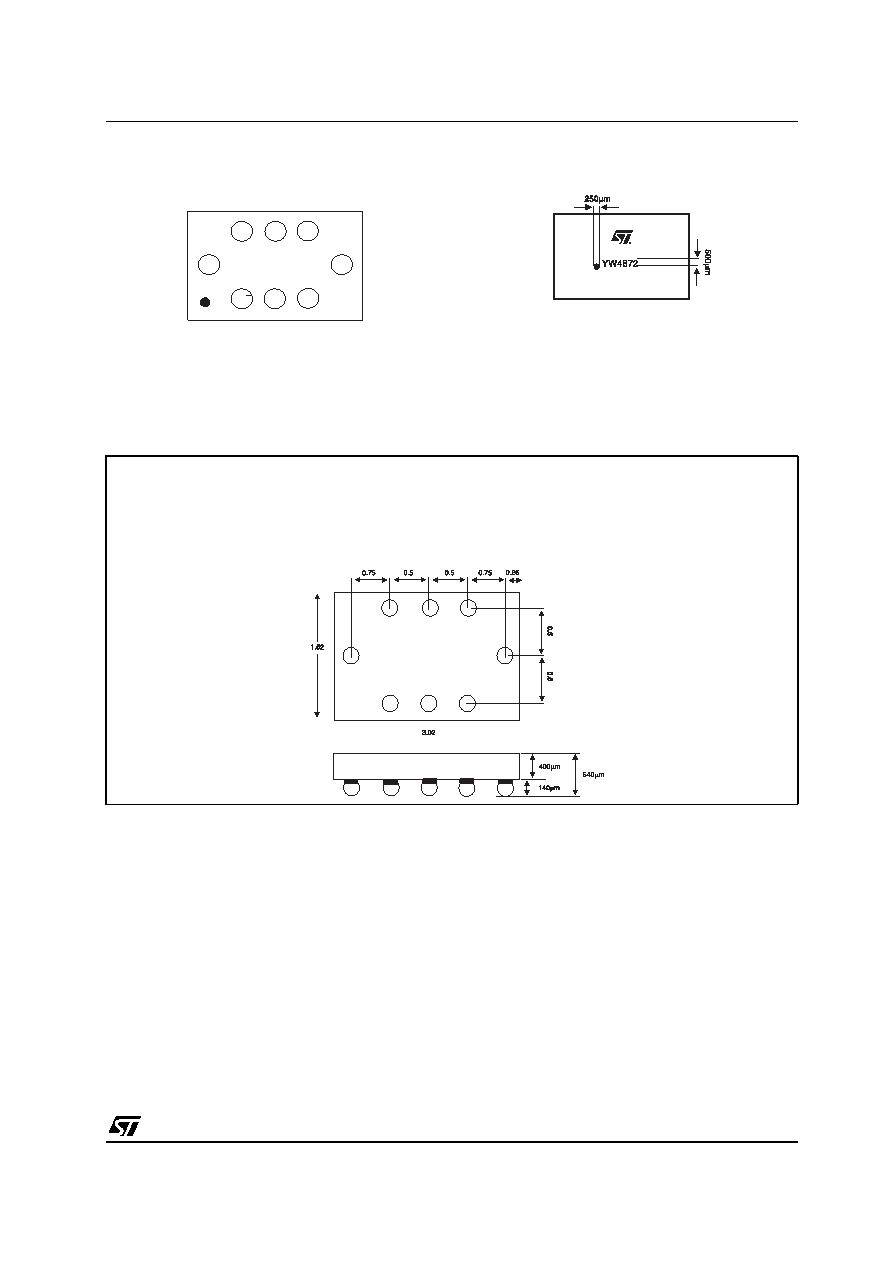
PIN OUT (top view)
MARKING (top view)
PACKAGE MECHANICAL DATA
FLIP CHIP - 8 BUMPS
12
3
76
5
8
4
GND
BYPASS
Vout2
STDBY
Vcc
Vout1
Vin
+
Vin
■ Balls are underneath
■ Y : Year
■ W : Week with two digits
■ Example : 1254872
■ Die size : (3.02mm±10%) x (1.52mm ±10%)
■ Die height (including bumps) : 540m ±50m
■ Bump height : 140m ±15m (i.e. bump diameter of 185m ±15m)
■ Silicon thickness : 400m±25m
■ Pitch: 500m ±10m and 750m±10m
Information furnished is believed to be accurate and reliable. However, STMicroelectronics assumes no responsibility for the
consequences of use of such information nor for any infringement of patents or other rights of third parties which may result from
its use. No license is granted by implication or otherwise under any patent or patent rights of STMicroelectronics. Specifications
mentioned in this publication are subject to change without notice. This publication supersedes and replaces all information
previously supplied. STMicroelectronics products are not authorized for use as critical components in life support devices or
systems without express written approval of STMicroelectronics.
The ST logo is a registered trademark of STMicroelectronics
2001 STMicroelectronics - Printed in Italy - All Rights Reserved
STMicroelectronics GROUP OF COMPANIES
Australia - Brazil - Canada - China - Finland - France - Germany - Hong Kong - India - Israel - Italy - Japan - Malaysia
Malta - Morocco - Singapore - Spain - Sweden - Switzerland - United Kingdom - United States
http://www.st.com
相关PDF资料 |
PDF描述 |
|---|---|
| TSH103ID | 3 CHANNEL, VIDEO AMPLIFIER, PDSO8 |
| TSH103IDT | 3 CHANNEL, VIDEO AMPLIFIER, PDSO8 |
| TSH120ICT | SPECIALTY CONSUMER CIRCUIT, PDSO6 |
| TSH122ICT | 1 CHANNEL, VIDEO AMPLIFIER, PDSO6 |
| TSH173IDT | SPECIALTY CONSUMER CIRCUIT, PDSO8 |
相关代理商/技术参数 |
参数描述 |
|---|---|
| TS487-2IQT | 制造商:未知厂家 制造商全称:未知厂家 功能描述:Amplifier. Other |
| TS487-2IST | 制造商:未知厂家 制造商全称:未知厂家 功能描述:Amplifier. Other |
| TS487-4 | 制造商:STMICROELECTRONICS 制造商全称:STMicroelectronics 功能描述:100mW STEREO HEADPHONE AMPLIFIER WITH STANDBY MODE |
| TS487-4IQT | 制造商:未知厂家 制造商全称:未知厂家 功能描述:Amplifier. Other |
| TS487-4IST | 制造商:未知厂家 制造商全称:未知厂家 功能描述:Amplifier. Other |
发布紧急采购,3分钟左右您将得到回复。