- 您现在的位置:买卖IC网 > PDF目录69533 > TS5A23167YZPR (TEXAS INSTRUMENTS INC) DUAL 1-CHANNEL, SGL POLE SGL THROW SWITCH, BGA8 PDF资料下载
参数资料
| 型号: | TS5A23167YZPR |
| 厂商: | TEXAS INSTRUMENTS INC |
| 元件分类: | 多路复用及模拟开关 |
| 英文描述: | DUAL 1-CHANNEL, SGL POLE SGL THROW SWITCH, BGA8 |
| 封装: | GREEN, DSBGA-8 |
| 文件页数: | 1/29页 |
| 文件大小: | 672K |
| 代理商: | TS5A23167YZPR |
当前第1页第2页第3页第4页第5页第6页第7页第8页第9页第10页第11页第12页第13页第14页第15页第16页第17页第18页第19页第20页第21页第22页第23页第24页第25页第26页第27页第28页第29页
www.ti.com
FEATURES
APPLICATIONS
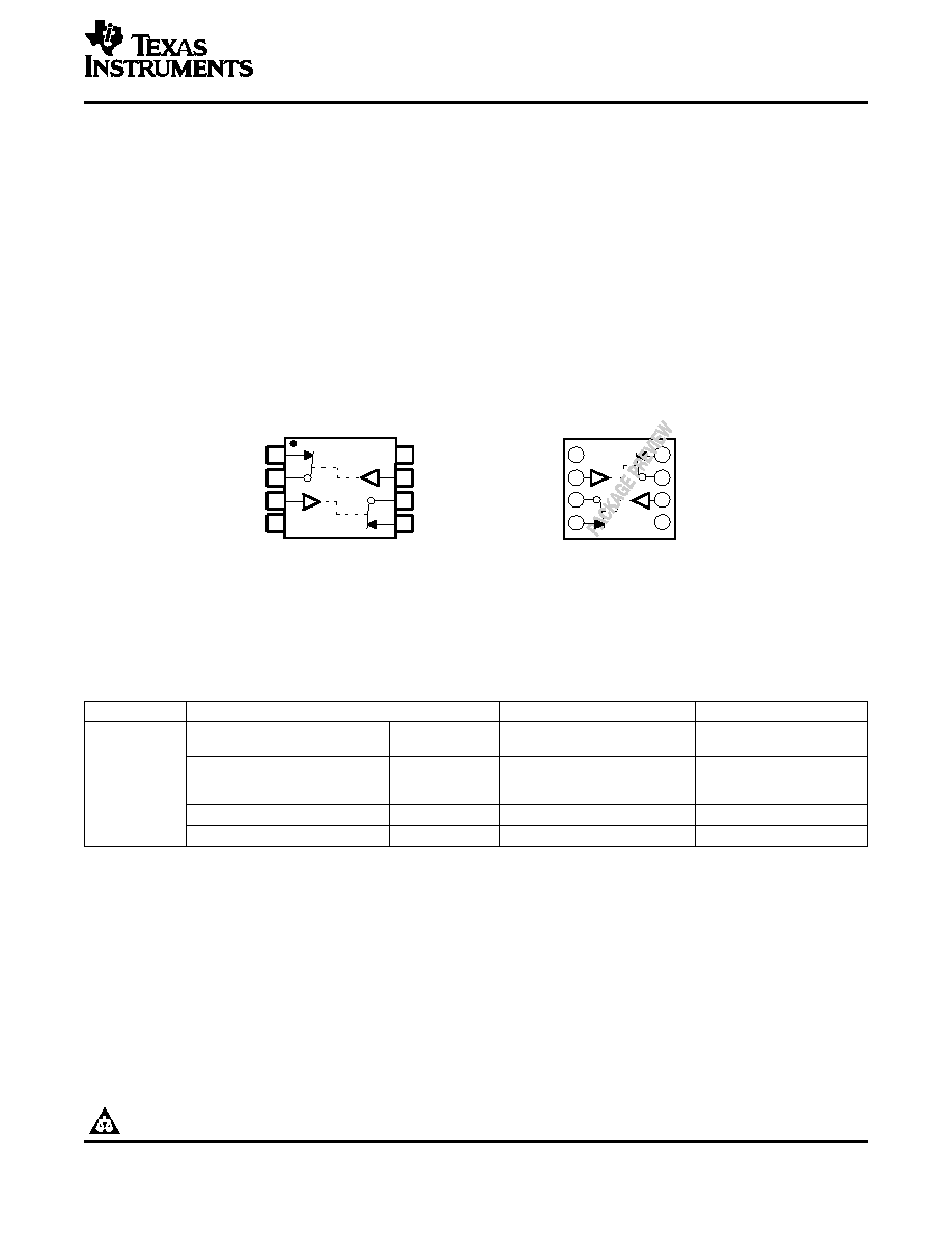
SSOP OR VSSOP PACKAGE
(TOP VIEW)
1
2
3
4
8
7
6
5
NC1
COM1
IN2
GND
COM2
IN1
V+
NC2
YEA, YEP, YZA, OR YZP PACKAGE
(BOTTOM VIEW)
GND
IN1
COM2
V+
2
3
4
8
7
5
6
IN2
COM1
NC1
NC2
1
DESCRIPTION/ORDERING INFORMATION
TS5A23167
0.9-
DUAL SPST ANALOG SWITCH
5-V/3.3-V 2-CHANNEL ANALOG SWITCH
SCDS195 – MAY 2005
Cell Phones
Isolation in Powered-Off Mode, V+ = 0
PDAs
Low ON-State Resistance (0.9
)
Portable Instrumentation
Control Inputs Are 5.5-V Tolerant
Audio and Video Signal Routing
Low Charge Injection
Low-Voltage Data Acquisition Systems
Low Total Harmonic Distortion (THD)
Communication Circuits
1.65-V to 5.5-V Single-Supply Operation
Modems
Latch-Up Performance Exceeds 100 mA Per
Hard Drives
JESD 78, Class II
Computer Peripherals
ESD Performance Tested Per JESD 22
Wireless Terminals and Peripherals
– 2000-V Human-Body Model(A114-B, Class II)
– 1000-V Charged-Device Model (C101)
The TS5A23167 is a dual single-pole single-throw (SPST) analog switch that is designed to operate from 1.65 V
to 5.5 V. The device offers a low ON-state resistance. The device has excellent total harmonic distortion (THD)
performance and consumes very low power. These features make this device suitable for portable audio
applications.
ORDERING INFORMATION
TA
PACKAGE(1)
ORDERABLE PART NUMBER
TOP-SIDE MARKING(2)
NanoStar – WCSP (DSBGA)
Tape and reel
TS5A23167YEPR
PACKAGE PREVIEW
0.23-mm Large Bump – YEP
NanoFree – WCSP (DSBGA)
0.23-mm Large Bump – YZP
Tape and reel
TS5A23167YZPR
PACKAGE PREVIEW
–40
°C to 85°C
(Pb-free)
SSOP – DCT
Tape and reel
TS5A23167DCTR
PACKAGE PREVIEW
VSSOP – DCU (Pb-free)
Tape and reel
TS5A23167DCUR
JAP_
(1)
Package drawings, standard packing quantities, thermal data, symbolization, and PCB design guidelines are available at
www.ti.com/sc/package.
(2)
DCT: The actual top-side marking has three additional characters that designate the year, month, and assembly/test site.
DCU: The acutal top-side marking has one additional character that designates the assembly/test site.
YEP/YZP: The actual top-side marking has three preceding characters to denote year, month, and sequence code, and one following
character to designate the assembly/test site. Pin 1 identifier indicates solder-bump composition (1 = SnPb,
= Pb-free).
Please be aware that an important notice concerning availability, standard warranty, and use in critical applications of Texas
Instruments semiconductor products and disclaimers thereto appears at the end of this data sheet.
PRODUCTION DATA information is current as of publication date.
Copyright 2005, Texas Instruments Incorporated
Products conform to specifications per the terms of the Texas
Instruments standard warranty. Production processing does not
necessarily include testing of all parameters.
相关PDF资料 |
PDF描述 |
|---|---|
| TS5A23167DCTR | DUAL 1-CHANNEL, SGL POLE SGL THROW SWITCH, PDSO8 |
| TS5A23167DCUR | DUAL 1-CHANNEL, SGL POLE SGL THROW SWITCH, PDSO8 |
| TS5A23167YEPR | DUAL 1-CHANNEL, SGL POLE SGL THROW SWITCH, BGA8 |
| TS5A26542YZTR | DUAL 1-CHANNEL, SGL POLE DOUBLE THROW SWITCH, BGA12 |
| TS5A3153DCURG4 | 1-CHANNEL, SGL POLE DOUBLE THROW SWITCH, PDSO8 |
相关代理商/技术参数 |
参数描述 |
|---|---|
| TS5A26466DCUR | 制造商:Texas Instruments 功能描述: |
| TS5A26542 | 制造商:TI 制造商全称:Texas Instruments 功能描述:0.75-W DUAL SPDT ANALOG SWITCH WITH INPUT LOGIC TRANSLATION |
| TS5A26542_10 | 制造商:TI 制造商全称:Texas Instruments 功能描述:0.75-?? DUAL SPDT ANALOG SWITCH WITH INPUT LOGIC TRANSLATION |
| TS5A26542YZTR | 功能描述:模拟开关 IC Dual SPDT Analog Sw RoHS:否 制造商:Texas Instruments 开关数量:2 开关配置:SPDT 开启电阻(最大值):0.1 Ohms 切换电压(最大): 开启时间(最大值): 关闭时间(最大值): 工作电源电压:2.7 V to 4.5 V 最大工作温度:+ 85 C 安装风格:SMD/SMT 封装 / 箱体:DSBGA-16 |
| TS5A3153 | 制造商:TI 制造商全称:Texas Instruments 功能描述:1-ohm SPDT ANALOG SWITCH 5-V/3.3-V SINGLE-CHANNEL 2:1 MULTIPLEXER/DEMULTIPLEXER |
发布紧急采购,3分钟左右您将得到回复。