- 您现在的位置:买卖IC网 > PDF目录136904 > TS80C51RD2-VCMR (ATMEL CORP) 8-BIT, 40 MHz, MICROCONTROLLER, PQFP64 PDF资料下载
参数资料
| 型号: | TS80C51RD2-VCMR |
| 厂商: | ATMEL CORP |
| 元件分类: | 微控制器/微处理器 |
| 英文描述: | 8-BIT, 40 MHz, MICROCONTROLLER, PQFP64 |
| 封装: | 1.40 MM HEIGHT, VQFP-64 |
| 文件页数: | 56/257页 |
| 文件大小: | 1840K |
| 代理商: | TS80C51RD2-VCMR |
第1页第2页第3页第4页第5页第6页第7页第8页第9页第10页第11页第12页第13页第14页第15页第16页第17页第18页第19页第20页第21页第22页第23页第24页第25页第26页第27页第28页第29页第30页第31页第32页第33页第34页第35页第36页第37页第38页第39页第40页第41页第42页第43页第44页第45页第46页第47页第48页第49页第50页第51页第52页第53页第54页第55页当前第56页第57页第58页第59页第60页第61页第62页第63页第64页第65页第66页第67页第68页第69页第70页第71页第72页第73页第74页第75页第76页第77页第78页第79页第80页第81页第82页第83页第84页第85页第86页第87页第88页第89页第90页第91页第92页第93页第94页第95页第96页第97页第98页第99页第100页第101页第102页第103页第104页第105页第106页第107页第108页第109页第110页第111页第112页第113页第114页第115页第116页第117页第118页第119页第120页第121页第122页第123页第124页第125页第126页第127页第128页第129页第130页第131页第132页第133页第134页第135页第136页第137页第138页第139页第140页第141页第142页第143页第144页第145页第146页第147页第148页第149页第150页第151页第152页第153页第154页第155页第156页第157页第158页第159页第160页第161页第162页第163页第164页第165页第166页第167页第168页第169页第170页第171页第172页第173页第174页第175页第176页第177页第178页第179页第180页第181页第182页第183页第184页第185页第186页第187页第188页第189页第190页第191页第192页第193页第194页第195页第196页第197页第198页第199页第200页第201页第202页第203页第204页第205页第206页第207页第208页第209页第210页第211页第212页第213页第214页第215页第216页第217页第218页第219页第220页第221页第222页第223页第224页第225页第226页第227页第228页第229页第230页第231页第232页第233页第234页第235页第236页第237页第238页第239页第240页第241页第242页第243页第244页第245页第246页第247页第248页第249页第250页第251页第252页第253页第254页第255页第256页第257页
149
ATmega8515(L)
2512K–AVR–01/10
Asynchronous Clock
Recovery
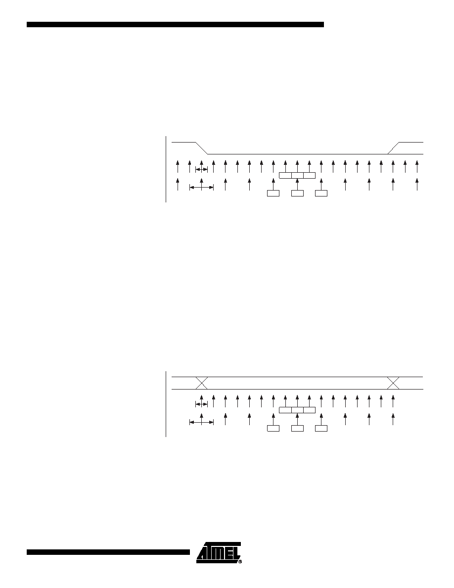
The clock recovery logic synchronizes internal clock to the incoming serial frames. Fig-
ure 68 illustrates the sampling process of the start bit of an incoming frame. The sample
rate is 16 times the baud rate for Normal mode, and eight times the baud rate for Double
Speed mode. The horizontal arrows illustrate the synchronization variation due to the
sampling process. Note the larger time variation when using the Double Speed mode
(U2X = 1) of operation. Samples denoted zero are samples done when the RxD line is
idle (i.e., no communication activity).
Figure 68. Start Bit Sampling
When the clock recovery logic detects a high (idle) to low (start) transition on the RxD
line, the start bit detection sequence is initiated. Let sample 1 denote the first zero-sam-
ple as shown in the figure. The clock recovery logic then uses samples 8, 9, and 10 for
Normal mode, and samples 4, 5, and 6 for Double Speed mode (indicated with sample
numbers inside boxes on the figure), to decide if a valid start bit is received. If two or
more of these three samples have logical high levels (the majority wins), the start bit is
rejected as a noise spike and the Receiver starts looking for the next high to low-transi-
tion. If however, a valid start bit is detected, the clock recovery logic is synchronized and
the data recovery can begin. The synchronization process is repeated for each start bit.
Asynchronous Data Recovery
When the Receiver clock is synchronized to the start bit, the data recovery can begin.
The data recovery unit uses a state machine that has 16 states for each bit in normal
mode and eight states for each bit in Double Speed mode. Figure 69 shows the sam-
pling of the data bits and the parity bit. Each of the samples is given a number that is
equal to the state of the recovery unit.
Figure 69. Sampling of Data and Parity Bit
The decision of the logic level of the received bit is taken by doing a majority voting of
the logic value to the three samples in the center of the received bit. The center samples
are emphasized on the figure by having the sample number inside boxes. The majority
voting process is done as follows: If two or all three samples have high levels, the
received bit is registered to be a logic 1. If two or all three samples have low levels, the
received bit is registered to be a logic 0. This majority voting process acts as a low pass
filter for the incoming signal on the RxD pin. The recovery process is then repeated until
a complete frame is received. Including the first stop bit. Note that the Receiver only
uses the first stop bit of a frame.
12
34
56
7
8
9
10
11
12
13
14
15
16
12
START
IDLE
0
BIT 0
3
123
4
5
678
12
0
RxD
Sample
(U2X = 0)
Sample
(U2X = 1)
12
34
56
7
8
9
10
11
12
13
14
15
16
1
BIT n
123
4
5
678
1
RxD
Sample
(U2X = 0)
Sample
(U2X = 1)
相关PDF资料 |
PDF描述 |
|---|---|
| TS80C51RD2-VIER | 8-BIT, 40 MHz, MICROCONTROLLER, PQFP44 |
| TS80C51RD2-VIB | 8-BIT, 40 MHz, MICROCONTROLLER, PQCC44 |
| TS87C51RC2-VCE | 8-BIT, OTPROM, 40 MHz, MICROCONTROLLER, PQFP44 |
| T14-14F | TIN FINISH, FORK TERMINAL |
| T10-6F | TIN FINISH, FORK TERMINAL |
相关代理商/技术参数 |
参数描述 |
|---|---|
| TS80C51RD2-VIA | 功能描述:IC MCU 8BIT 768BYTE 40MHZ 40-DIP RoHS:否 类别:集成电路 (IC) >> 嵌入式 - 微控制器, 系列:80C 标准包装:9 系列:87C 核心处理器:8051 芯体尺寸:8-位 速度:40/20MHz 连通性:UART/USART 外围设备:POR,WDT 输入/输出数:32 程序存储器容量:32KB(32K x 8) 程序存储器类型:OTP EEPROM 大小:- RAM 容量:256 x 8 电压 - 电源 (Vcc/Vdd):4.5 V ~ 5.5 V 数据转换器:- 振荡器型:内部 工作温度:0°C ~ 70°C 封装/外壳:40-DIP(0.600",15.24mm) 包装:管件 |
| TS80C51RD2-VIAD | 制造商:未知厂家 制造商全称:未知厂家 功能描述:8-Bit Microcontroller |
| TS80C51RD2-VIB | 功能描述:IC MCU 8BIT 768BYTE 40MHZ 44PLCC RoHS:否 类别:集成电路 (IC) >> 嵌入式 - 微控制器, 系列:80C 标准包装:1,500 系列:AVR® ATtiny 核心处理器:AVR 芯体尺寸:8-位 速度:16MHz 连通性:I²C,LIN,SPI,UART/USART,USI 外围设备:欠压检测/复位,POR,PWM,温度传感器,WDT 输入/输出数:16 程序存储器容量:8KB(4K x 16) 程序存储器类型:闪存 EEPROM 大小:512 x 8 RAM 容量:512 x 8 电压 - 电源 (Vcc/Vdd):2.7 V ~ 5.5 V 数据转换器:A/D 11x10b 振荡器型:内部 工作温度:-40°C ~ 125°C 封装/外壳:20-SOIC(0.295",7.50mm 宽) 包装:带卷 (TR) |
| TS80C51RD2-VIBB | 制造商:未知厂家 制造商全称:未知厂家 功能描述:8-Bit Microcontroller |
| TS80C51RD2-VIBD | 制造商:未知厂家 制造商全称:未知厂家 功能描述:8-Bit Microcontroller |
发布紧急采购,3分钟左右您将得到回复。