- 您现在的位置:买卖IC网 > PDF目录98301 > TSA1002CF (STMICROELECTRONICS) 1-CH 10-BIT PROPRIETARY METHOD ADC, PARALLEL ACCESS, PQFP48 PDF资料下载
参数资料
| 型号: | TSA1002CF |
| 厂商: | STMICROELECTRONICS |
| 元件分类: | ADC |
| 英文描述: | 1-CH 10-BIT PROPRIETARY METHOD ADC, PARALLEL ACCESS, PQFP48 |
| 封装: | 7 X 7 MM, PLASTIC, TQFP-48 |
| 文件页数: | 9/20页 |
| 文件大小: | 236K |
| 代理商: | TSA1002CF |
Obsolete
Product(s)
- Obsolete
Product(s)
TSA1002
17/20
NO
T
FOR
NEW
DESI
G
N
Clock input
The quality of your converter is very dependant on
your clock input accuracy, in terms of aperture
jitter; the use of low jitter crystal controlled
oscillator is recommended.
The clock power supplies must be separated from
the ADC output ones to avoid digital noise
modulation at the output.
It is recommended to keep the circuit clocked, to
avoid random states, before applying the supply
voltages.
Layout precautions
To use the ADC circuits in the best manner at high
frequencies, some precautions have to be taken
for power supplies:
- First of all, the implementation of 4 separate
proper supplies and ground planes (analog,
digital, internal and external buffer ones) on the
PCB is recommended for high speed circuit
applications to provide low inductance and low
resistance common return.
The separation of the analog signal from the
digital part is essential to prevent noise from
coupling onto the input signal.
- Power supply bypass capacitors must be placed
as close as possible to the IC pins in order to
improve high frequency bypassing and reduce
harmonic distortion.
- Proper termination of all inputs and outputs is
needed; with output termination resistors, the
amplifier load will be only resistive and the stability
of the amplifier will be improved. All leads must be
wide and as short as possible especially for the
analog input in order to decrease parasitic
capacitance and inductance.
- To keep the capacitive loading as low as
possible at digital outputs, short lead lengths of
routing are essential to minimize currents when
the output changes. To minimize this output
capacitance, buffers or latches close to the output
pins will relax this constraint.
- Choose component sizes as small as possible
(SMD).
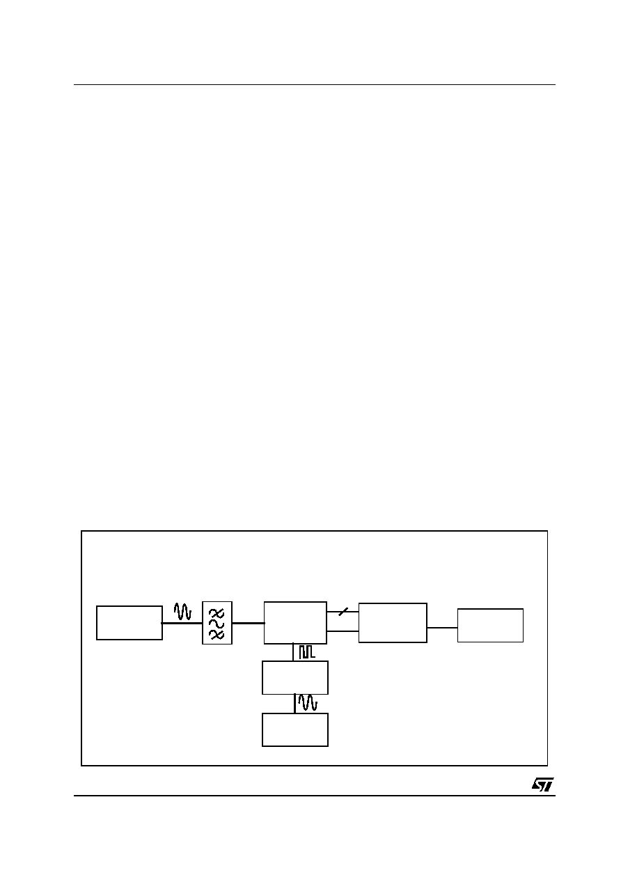
EVAL1002 evaluation board
The characterization of the board has been made
with a fully ADC devoted test bench as shown on
Figure 11. The analog signal must be filtered to be
very pure.
The dataready signal is the acquisition clock of the
logic analyzer.
The ADC digital outputs are latched by the
74LCX573 octal buffers.
All characterization measurement has been made
with an input amplitude of +0.2dB for static
parameters and -0.5dB for dynamic parameters.
Figure 11 : Analog to Digital Converter characterization bench
Sine Wave
Generator
HP8644
ADC
evaluation
board
Pulse
Generator
Logic
Analyzer
Sine Wave
Generator
HP8644
HP8133
Vin
Clk
Data
Clk
PC
相关PDF资料 |
PDF描述 |
|---|---|
| TSA1002IF | 1-CH 10-BIT PROPRIETARY METHOD ADC, PARALLEL ACCESS, PQFP48 |
| TSA1002IFT | 1-CH 10-BIT PROPRIETARY METHOD ADC, PARALLEL ACCESS, PQFP48 |
| TSA1005-20IFT | 2-CH 10-BIT PROPRIETARY METHOD ADC, PARALLEL ACCESS, PQFP48 |
| TSA1005-40IFT | 2-CH 10-BIT PROPRIETARY METHOD ADC, PARALLEL ACCESS, PQFP48 |
| TSA1005I-40IF | 2-CH 10-BIT PROPRIETARY METHOD ADC, PARALLEL ACCESS, PQFP48 |
相关代理商/技术参数 |
参数描述 |
|---|---|
| TSA1002CFT | 制造商:STMICROELECTRONICS 制造商全称:STMicroelectronics 功能描述:10-BIT, 50MSPS, 50mW A/D CONVERTER |
| TSA1002IF | 制造商:STMICROELECTRONICS 制造商全称:STMicroelectronics 功能描述:10-BIT, 50MSPS, 50mW A/D CONVERTER |
| TSA1002IFT | 制造商:STMICROELECTRONICS 制造商全称:STMicroelectronics 功能描述:10-BIT, 50MSPS, 50mW A/D CONVERTER |
| TSA1005 | 制造商:STMICROELECTRONICS 制造商全称:STMicroelectronics 功能描述:DUAL-CHANNEL, 10-BIT, 20/40MSPS A/D CONVERTER |
| TSA1005-20IF | 制造商:STMicroelectronics 功能描述:ADC DUAL PIPELINED 20MSPS 10-BIT PARALLEL 48TQFP - Trays |
发布紧急采购,3分钟左右您将得到回复。