- 您现在的位置:买卖IC网 > PDF目录98301 > TSC2003I (TEXAS INSTRUMENTS INC) 3-CH 12-BIT SUCCESSIVE APPROXIMATION ADC, SERIAL ACCESS, PDSO16 PDF资料下载
参数资料
| 型号: | TSC2003I |
| 厂商: | TEXAS INSTRUMENTS INC |
| 元件分类: | ADC |
| 英文描述: | 3-CH 12-BIT SUCCESSIVE APPROXIMATION ADC, SERIAL ACCESS, PDSO16 |
| 封装: | PLASTIC, TSSOP-16 |
| 文件页数: | 10/20页 |
| 文件大小: | 309K |
| 代理商: | TSC2003I |
TSC2003
18
SBAS162A
www.ti.com
PENIRQ output is HIGH. While in the power-down mode,
with PD0 = 0, the Y– driver is ON and connected to GND,
and the PENIRQ output is connected to the X+ input. When
the panel is touched, the X+ input is pulled to ground
through the touch screen, and PENIRQ output goes LOW
due to the current path through the panel to GND, initiating
an interrupt to the processor. During the measurement cycle
for X-, Y-, and Z-Position, the X+ input will be disconnected
from the PENIRQ pull-down transistor to eliminate any
leakage current from the pull-up resistor to flow through the
touch screen, thus causing no errors.
In addition to the measurement cycles for X-, Y-, and Z-position,
commands which activate the X-drivers, Y-drivers, Y+ and
X-drivers without performing a measurement also disconnect the
X+ input from the PENIRQ pull-down transistor and disable the
pen-interrupt output function regardless of the value of the PD0
bit. Under these conditions, the PENIRQ output will be forced
LOW. Furthermore, if the last command byte written to the
TSC2003 contains PD0 = 1, the pen-interrupt output function
will be disabled and will not be able to detect when the panel is
touched. In order to re-enable the pen-interrupt output function
under these circumstances, a command byte needs to be written
to the TSC2003 with PD0 = 0.
Once the bus master sends the address byte with R/W = 0
(see Figure 10) and the TSC2003 sends an acknowledge, the
pen-interrupt function is disabled. If the command which
follows the address byte has PD0 = 0, then the pen-interrupt
function will be enabled at the end of a conversion. This is
approximately 10
s (12-bit mode) or 7s (8-bit mode) after
the TSC2003 receives a STOP/START condition following
the reception of a command byte (see Figures 12 and 14 for
further details of when the conversion cycle begins).
In both cases listed above, it is recommended that the master
processor mask the interrupt which the PENIRQ is associ-
ated with whenever the host writes to the TSC2003. This
will prevent false triggering of interrupts when the PENIRQ
line is disabled in the cases listed above.
For optimum performance, care should be taken with the
physical layout of the TSC2003 circuitry. The basic SAR
architecture is sensitive to glitches or sudden changes on the
power supply, reference, ground connections, and digital
inputs that occur just prior to latching the output of the
analog comparator. Therefore, during any single conversion
for an n-bit SAR converter, there are n “windows” in which
large external transient voltages can easily affect the conver-
sion result. Such glitches might originate from switching
power supplies, nearby digital logic, and high-power de-
vices. The degree of error in the digital output depends on
the reference voltage, layout, and the exact timing of the
external event. The error can change if the external event
changes in time with respect to the SCL input.
With this in mind, power to the TSC2003 should be clean and
well bypassed. A 0.1
F ceramic bypass capacitor should be
placed as close to the device as possible. In addition, a 1
F to
10
F capacitor may also be needed if the impedance of the
connection between +VDD and the power supply is high.
A bypass capacitor is generally not needed on the VREF pin
because the internal reference is buffered by an internal op
amp. If an external reference voltage originates from an op
amp, make sure that it can drive any bypass capacitor that is
used without oscillation.
The TSC2003 architecture offers no inherent rejection of noise
or voltage variation in regards to using an external reference
input. This is of particular concern when the reference input is
tied to the power supply. Any noise and ripple from the supply
will appear directly in the digital results. While high-frequency
noise can be filtered out, voltage variation due to line frequency
(50Hz or 60Hz) can be difficult to remove.
The GND pin should be connected to a clean ground point. In
many cases, this will be the “analog” ground. Avoid connec-
tions which are too near the grounding point of a microcontroller
or digital signal processor. If needed, run a ground trace directly
from the converter to the power-supply entry point. The ideal
layout will include an analog ground plane dedicated to the
converter and associated analog circuitry.
In the specific case of use with a resistive touch screen, care
should be taken with the connection between the converter
and the touch screen. Since resistive touch screens have
fairly low resistance, the interconnection should be as short
and robust as possible. Longer connections will be a source
of error, much like the on-resistance of the internal switches.
Likewise, loose connections can be a source of error when
the contact resistance changes with flexing or vibrations.
As indicated previously, noise can be a major source of error
in touch screen applications (e.g., applications that require a
backlit LCD panel). This EMI noise can be coupled through
the LCD panel to the touch screen and cause “flickering” of
the converted data. Several things can be done to reduce this
error, such as utilizing a touch screen with a bottom-side
metal layer connected to ground. This will couple the major-
ity of noise to ground. Additionally, filtering capacitors from
Y+, Y–, X+, and X– to ground can also help.
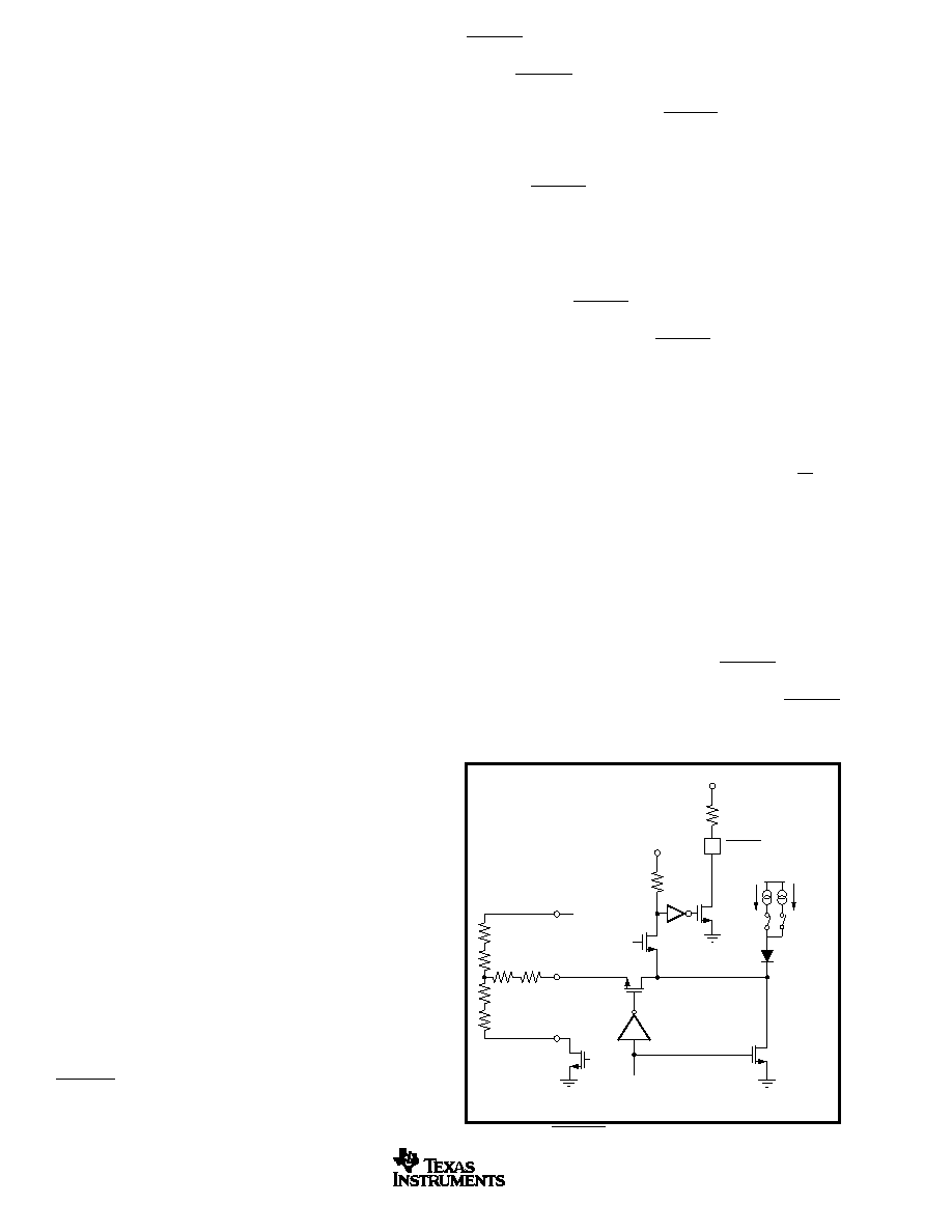
PENIRQ OUTPUT
The pen-interrupt output function is shown in Figure 16. By
connecting a pull-up resistor to VDD (typically 100k), the
PENIRQ
V
DD
10k
30k
to 100k
ON
Y+ or X+ drivers on,
or TEMP0, TEMP1
measurements activated
Y+
X+
Y–
TEMP0
TEMP1
TEMP
DIODE
HIGH except
when TEMP0,
TEMP1 activated
V
DD
V
DD
FIGURE 16. PENIRQ Functional Block Diagram.
相关PDF资料 |
PDF描述 |
|---|---|
| TSC2003IR | 3-CH 12-BIT SUCCESSIVE APPROXIMATION ADC, SERIAL ACCESS, PDSO16 |
| TSC2008IRGVR | SPECIALTY CONSUMER CIRCUIT, PQCC16 |
| TSC2008IRGVT | SPECIALTY CONSUMER CIRCUIT, PQCC16 |
| TSC2008IYZGR | SPECIALTY CONSUMER CIRCUIT, BGA12 |
| TSC2008IYZGT | SPECIALTY CONSUMER CIRCUIT, BGA12 |
相关代理商/技术参数 |
参数描述 |
|---|---|
| TSC2003IPW | 功能描述:触摸屏转换器和控制器 4-wire Touch Screen Controller RoHS:否 制造商:Microchip Technology 类型:Resistive Touch Controllers 输入类型:3 Key 数据速率:140 SPS 分辨率:10 bit 接口类型:4-Wire, 5-Wire, 8-Wire, I2C, SPI 电源电压:2.5 V to 5.25 V 电源电流:17 mA 工作温度:- 40 C to + 85 C 封装 / 箱体:SSOP-20 |
| TSC2003IPWG4 | 功能描述:触摸屏转换器和控制器 4-wire Touch Screen Controller RoHS:否 制造商:Microchip Technology 类型:Resistive Touch Controllers 输入类型:3 Key 数据速率:140 SPS 分辨率:10 bit 接口类型:4-Wire, 5-Wire, 8-Wire, I2C, SPI 电源电压:2.5 V to 5.25 V 电源电流:17 mA 工作温度:- 40 C to + 85 C 封装 / 箱体:SSOP-20 |
| TSC2003IPWR | 功能描述:触摸屏转换器和控制器 4-wire Touch Screen Controller RoHS:否 制造商:Microchip Technology 类型:Resistive Touch Controllers 输入类型:3 Key 数据速率:140 SPS 分辨率:10 bit 接口类型:4-Wire, 5-Wire, 8-Wire, I2C, SPI 电源电压:2.5 V to 5.25 V 电源电流:17 mA 工作温度:- 40 C to + 85 C 封装 / 箱体:SSOP-20 |
| TSC2003IPWR | 制造商:Texas Instruments 功能描述:Controller IC |
| TSC2003IPWRG4 | 功能描述:触摸屏转换器和控制器 4-wire Touch Screen Controller RoHS:否 制造商:Microchip Technology 类型:Resistive Touch Controllers 输入类型:3 Key 数据速率:140 SPS 分辨率:10 bit 接口类型:4-Wire, 5-Wire, 8-Wire, I2C, SPI 电源电压:2.5 V to 5.25 V 电源电流:17 mA 工作温度:- 40 C to + 85 C 封装 / 箱体:SSOP-20 |
发布紧急采购,3分钟左右您将得到回复。