- 您现在的位置:买卖IC网 > PDF目录365968 > TSC21020F-20SAP833 FPGA, CYCLONE III, 40K LE, 324FBGA Programmable Logic Type:FPGA; Logic IC function:FPGA; Logic IC family:Cyclone III; Logic IC Base Number:3; I/O lines, No. of:195; PDF资料下载
参数资料
| 型号: | TSC21020F-20SAP833 |
| 英文描述: | FPGA, CYCLONE III, 40K LE, 324FBGA Programmable Logic Type:FPGA; Logic IC function:FPGA; Logic IC family:Cyclone III; Logic IC Base Number:3; I/O lines, No. of:195; |
| 中文描述: | 数字信号处理器| 32位|的CMOS | RAD数据通信硬|美巡赛| 223PIN |陶瓷 |
| 文件页数: | 12/51页 |
| 文件大小: | 763K |
| 代理商: | TSC21020F-20SAP833 |
第1页第2页第3页第4页第5页第6页第7页第8页第9页第10页第11页当前第12页第13页第14页第15页第16页第17页第18页第19页第20页第21页第22页第23页第24页第25页第26页第27页第28页第29页第30页第31页第32页第33页第34页第35页第36页第37页第38页第39页第40页第41页第42页第43页第44页第45页第46页第47页第48页第49页第50页第51页
12
TSC21020F
4153F
–
AERO
–
06/03
DMRD
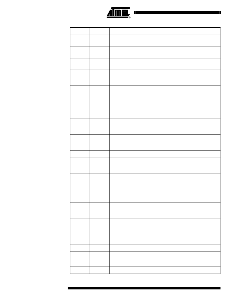
O
Data Memory Read strobe. This pin is asserted when the TSC21020F
reads from data memory.
DMWR
O
Data Memory Write strobe. This pin is asserted when the TSC21020F
writes to data memory.
DMACK
I/S
Data Memory Acknowledge. An external device de-asserts this input to
add wait states to a memory access.
DMPAGE
O
Data Memory Page Boundary. The TSC21020F asserts this pin to
signal that a data memory page boundary has been crossed. Memory
pages must be defined in the memory control registers.
DMTS
I/S
Data Memory Three-State Control. DMTS places the data memory
address, data, selects, and strobes in a high-impedance state. If DMTS
is asserted while
à
DM access is occurring, the processor will halt and
the memory access will not be completed. DMACK must be asserted
for at least one cycle when DMTS is de-asserted to allow any pending
memory access to complete properly. DMTS should only be asserted
(low) during an active memory access cycle.
CLKIN
I
External clock input to the TSC21020F. The instruction cycle rate is
equal to CLKIN. CLKIN may not be halted, changed, or operated below
the specified frequency.
RESET
I/A
Sets the TSC21020F to a known state and begins execution at the
program memory location specified by the hardware reset vector
(address). This input must be asserted (low) at power-up.
IRQ
3-0
I/A
Interrupt request lines; may be either edge-riggered or level-sensitive.
FLAG
3-0
I/O/A
External Flags. Each is configured via control bits as either an input or
output. As an input, it can be tested as a condition. As an output, it can
be used to signal external peripherals.
BR
I/A
Bus Request. Used by an external device to request control of the
memory interface. When BR is asserted, the processor halts execution
after completion of the current cycle, places all memory data,
addresses, selects, and strobes in a high-impedance state, and
asserts BG. The processor continues normal operation when BR is
released.
BG
O
Bus Grant. Acknowledges a bus request (BR), indicating that the
external device may take control of the memory interface. BG is
asserted (held low) until BR is released.
TIMEXP
O
Timer Expired. Asserted for four cycles when the value of TCOUNT is
decremented to zero.
RCOMP
Not available
Can be set to any voltage level.
EVDD
P
Power supply (for output drivers), nominally + 5V dc (10 pins).
EGND
G
Power supply return (for output drivers); (16 pins).
IVDD
P
Power supply (for internal circuitry), nominally + 5V dc (4 pins).
IGND
G
Power supply return (for internal circuitry); (7 pins).
Pin Name
Type
Function
相关PDF资料 |
PDF描述 |
|---|---|
| TSC21020F-20SASB | IC CYCLONE III FPGA 40K 324 FBGA |
| TSC21020F-20SASC | IC CYCLONE III FPGA 40K 484FBGA |
| TSC21020F-20SASL1 | IC CYCLONE III FPGA 40K 484FBGA |
| TSC21020F-20SASL2 | IC CYCLONE III FPGA 40K 484 FBGA |
| TSC21020F-20SASL3 | IC CYCLONE III FPGA 40K 780FBGA |
相关代理商/技术参数 |
参数描述 |
|---|---|
| TSC21020F-20SASB | 制造商:未知厂家 制造商全称:未知厂家 功能描述:DSP|32-BIT|CMOS| RAD HARD|PGA|223PIN|CERAMIC |
| TSC21020F-20SASC | 制造商:未知厂家 制造商全称:未知厂家 功能描述:DSP|32-BIT|CMOS| RAD HARD|PGA|223PIN|CERAMIC |
| TSC21020F-20SASL1 | 制造商:未知厂家 制造商全称:未知厂家 功能描述:DSP|32-BIT|CMOS| RAD HARD|PGA|223PIN|CERAMIC |
| TSC21020F-20SASL2 | 制造商:未知厂家 制造商全称:未知厂家 功能描述:DSP|32-BIT|CMOS| RAD HARD|PGA|223PIN|CERAMIC |
| TSC21020F-20SASL3 | 制造商:未知厂家 制造商全称:未知厂家 功能描述:DSP|32-BIT|CMOS| RAD HARD|PGA|223PIN|CERAMIC |
发布紧急采购,3分钟左右您将得到回复。