参数资料
| 型号: | TSC80251G2D-16CB |
| 厂商: | Atmel |
| 文件页数: | 38/77页 |
| 文件大小: | 0K |
| 描述: | IC MCU 8BIT 16MHZ HI SPD 44-PLCC |
| 标准包装: | 27 |
| 系列: | 8x251 |
| 核心处理器: | C251 |
| 芯体尺寸: | 8/16-位 |
| 速度: | 16MHz |
| 连通性: | EBI/EMI,I²C,Microwire,SPI,UART/USART |
| 外围设备: | POR,PWM,WDT |
| 输入/输出数: | 32 |
| 程序存储器类型: | ROMless |
| RAM 容量: | 1K x 8 |
| 电压 - 电源 (Vcc/Vdd): | 4.5 V ~ 5.5 V |
| 振荡器型: | 内部 |
| 工作温度: | 0°C ~ 70°C |
| 封装/外壳: | 44-LCC(J 形引线) |
| 包装: | 管件 |
第1页第2页第3页第4页第5页第6页第7页第8页第9页第10页第11页第12页第13页第14页第15页第16页第17页第18页第19页第20页第21页第22页第23页第24页第25页第26页第27页第28页第29页第30页第31页第32页第33页第34页第35页第36页第37页当前第38页第39页第40页第41页第42页第43页第44页第45页第46页第47页第48页第49页第50页第51页第52页第53页第54页第55页第56页第57页第58页第59页第60页第61页第62页第63页第64页第65页第66页第67页第68页第69页第70页第71页第72页第73页第74页第75页第76页第77页
43
AT/TSC8x251G2D
4135F–8051–11/06
PSEN# and the other control signals have to be released to complete a sequence of
programming operations or a sequence of programming and verifying operations.
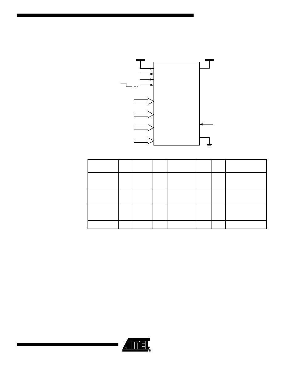
Figure 6.
Setup for Programming
Table 36.
Programming Modes
Notes: 1. Signature Bytes are not user-programmable.
2. The ALE/PROG# pulse waveform is shown in Figure 23 page 59.
Verify Algorithm
Figure 7 shows the hardware setup needed to verify the TSC87251G2D
EPROM/OTPROM or TSC83251G2D ROM areas:
The chip has to be put under reset and maintained in this state until the completion
of the verifying sequence.
PSEN# and the other control signals (ALE and Port 0) have to be set to a high level.
Then PSEN# has to be to forced to a low level after two clock cycles or more and it
has to be maintained in this state until the completion of the verifying sequence (see
below).
The voltage on the EA# pin must be set to VDD and ALE must be set to a high level.
The Verifying Mode is selected according to the code applied on Port 0. It has to be
applied until the completion of this verifying operation.
The verifying address is applied on Ports 1 and 3 which are respectively the MSB
and the LSB of the address.
ROM Area
(1)
RST
EA#/VPP
PSEN
#
ALE/PROG#
(2)
P0
P2
P1(MSB) P3(LSB)
On-chip Code
Memory
1VPP
0
1 Pulse
68h
Data
16-bit Address
0000h-7FFFh (32
kilobytes)
Configuration
Bytes
1VPP
0
1 Pulse
69h
Data
CONFIG0: FFF8h
CONFIG1: FFF9h
Lock Bits
1
VPP
0
1 Pulse
6Bh
X
LB0: 0001h
LB1: 0002h
LB2: 0003h
Encryption Array
1
VPP
0
1 Pulse
6Ch
Data 0000h-007Fh
VDD
PSEN#
ALE/PROG#
EA#/VPP
XTAL1
VDD
4 to 12 MHz
RST
VPP
100 ms pulses
VSS/VSS1/VSS2
Mode
VDD
A[7:0]
A[14:8]
Data
P0[7:0]
P3[7:0]
P1[7:0]
P2[7:0]
TSC87251G2D
相关PDF资料 |
PDF描述 |
|---|---|
| 52610-2690 | CONN FFC/FPC 26POS 1MM VERT SMD |
| TSC80251G2D-24IB | IC MCU 8BIT 24MHZ HI SPD 44-PLCC |
| PIC16F84A-04/P | IC MCU FLASH 1KX14 EE 18DIP |
| DSPIC30F2020-20E/MM | IC DSPIC MCU/DSP 12K 28QFN |
| ATTINY13V-10SSI | IC MCU AVR 1K FLASH 10MHZ 8SOIC |
相关代理商/技术参数 |
参数描述 |
|---|---|
| TSC80251G2D-16CBR | 功能描述:IC MCU 8BIT 16MHZ HI SPD 44-PLCC RoHS:否 类别:集成电路 (IC) >> 嵌入式 - 微控制器, 系列:8x251 标准包装:1,500 系列:AVR® ATtiny 核心处理器:AVR 芯体尺寸:8-位 速度:16MHz 连通性:I²C,LIN,SPI,UART/USART,USI 外围设备:欠压检测/复位,POR,PWM,温度传感器,WDT 输入/输出数:16 程序存储器容量:8KB(4K x 16) 程序存储器类型:闪存 EEPROM 大小:512 x 8 RAM 容量:512 x 8 电压 - 电源 (Vcc/Vdd):2.7 V ~ 5.5 V 数据转换器:A/D 11x10b 振荡器型:内部 工作温度:-40°C ~ 125°C 封装/外壳:20-SOIC(0.295",7.50mm 宽) 包装:带卷 (TR) |
| TSC80251G2D-24CB | 功能描述:IC C251 MCU ROMLESS 5V 44PLCC RoHS:否 类别:集成电路 (IC) >> 嵌入式 - 微控制器, 系列:8x251 标准包装:1,500 系列:AVR® ATtiny 核心处理器:AVR 芯体尺寸:8-位 速度:16MHz 连通性:I²C,LIN,SPI,UART/USART,USI 外围设备:欠压检测/复位,POR,PWM,温度传感器,WDT 输入/输出数:16 程序存储器容量:8KB(4K x 16) 程序存储器类型:闪存 EEPROM 大小:512 x 8 RAM 容量:512 x 8 电压 - 电源 (Vcc/Vdd):2.7 V ~ 5.5 V 数据转换器:A/D 11x10b 振荡器型:内部 工作温度:-40°C ~ 125°C 封装/外壳:20-SOIC(0.295",7.50mm 宽) 包装:带卷 (TR) |
| TSC80251G2D-24CBR | 制造商:Atmel Corporation 功能描述:MCU 8-bit/16-bit 8x251 C251 CISC ROMLess 3.3V/5V 44-Pin PLCC |
| TSC80251G2D-24CE | 功能描述:IC C251 MCU ROMLESS 5V 44VQFP RoHS:否 类别:集成电路 (IC) >> 嵌入式 - 微控制器, 系列:8x251 标准包装:1,500 系列:AVR® ATtiny 核心处理器:AVR 芯体尺寸:8-位 速度:16MHz 连通性:I²C,LIN,SPI,UART/USART,USI 外围设备:欠压检测/复位,POR,PWM,温度传感器,WDT 输入/输出数:16 程序存储器容量:8KB(4K x 16) 程序存储器类型:闪存 EEPROM 大小:512 x 8 RAM 容量:512 x 8 电压 - 电源 (Vcc/Vdd):2.7 V ~ 5.5 V 数据转换器:A/D 11x10b 振荡器型:内部 工作温度:-40°C ~ 125°C 封装/外壳:20-SOIC(0.295",7.50mm 宽) 包装:带卷 (TR) |
| TSC80251G2D-24CED | 制造商:TEMIC 制造商全称:TEMIC Semiconductors 功能描述:8/16-bit Microcontroller with Serial Communication Interfaces |
发布紧急采购,3分钟左右您将得到回复。