- 您现在的位置:买卖IC网 > Datasheet目录58 > TSL3301CL (AMS-TAOS USA Inc)IC LINEAR SENSOR ARRAY 8CHIPLED Datasheet资料下载
参数资料
| 型号: | TSL3301CL |
| 厂商: | AMS-TAOS USA Inc |
| 文件页数: | 5/21页 |
| 文件大小: | 659K |
| 描述: | IC LINEAR SENSOR ARRAY 8CHIPLED |
| 标准包装: | 1 |
| 系列: | * |
| 其它名称: | TSL3301-CLDKR |
TSL3301CL
102 ?1 LINEAR OPTICAL SENSOR ARRAY
WITH ANALOG-TO-DIGITAL CONVERTER
TAOS141 JULY 2011
4
r
r
Copyright E 2011, TAOS Inc.
The LUMENOLOGY r Company
www.taosinc.com
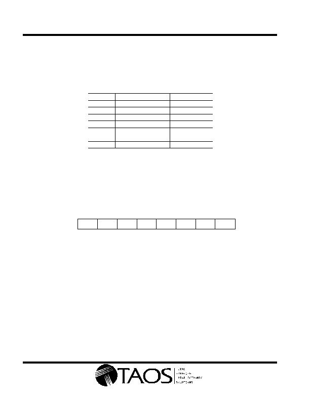
Register Address Map
The TSL3301CL contains seven registers as defined in Table 2. Data in these registers may be written to or read
from using the REGWrite and REGRead commands. Three registers control the gain of the analog-to-digital
converters (ADC). Three other registers allow the offset of the system to be adjusted. Together the gain and
offset registers are used to maximize the achievable dynamic range.
Table 2. Register Address Map
ADDRESS
REGISTER DESCRIPTION
REGISTER WIDTH
0x00
Left (pixels 033) offset
8
0x01
Left (pixels 033) gain
5
0x02
Center (pixels 3467) offset
8
0x03
Center (pixels 3467) gain
5
0x04
Right (pixels 68101) offset
8
0x05
Right (pixels 68101) gain
5
0x1F
Mode
8
The offset registers are 8-bit sign-magnitude values and the gain registers are 5-bit values. The programmed
offset correction is applied to the sampled energy, and then the gain is applied. (i.e., the gain will affect the offset
correction.) These registers allow the user to maximize the dynamic range achievable in the given system.
The last register is the mode register. Bits in this register select the sleep mode as well as options for multichip
arrays and production testing. Note that test and multichip options do not apply to the 8-pin packaged device.
Users should always write 0s into the production test and multichip control bits.
0
7
0x1F
6
5
4
3
2
1
P2
MODE
0
0
SLP
P1
P0
C1
C0
SLP = Sleep Mode:
1 places device into sleep mode
0 places device in normal operating mode
C1, C0 are Reserved (should be written 0)
P2 to P0 are factory test bits (should be written 0)
Figure 1. Mode Register Bit Assignments
相关PDF资料 |
PDF描述 |
|---|---|
| TXM-418-LR_ | TRANSMITTER 418MHZ LR SERIES |
| TXM-900-HP3-SPS | TRANSMTR RF 902-928MHZ 8P/100S |
| VJ3505M011SXMSRA0 | ANTENNA 470-860MHZ UHF SMD |
| VJ5301M868MXBSR | RF ANTENNA |
| VJ5301M915MXBSR | RF ANTENNA |
相关代理商/技术参数 |
参数描述 |
|---|---|
| TSL3301EVM | 功能描述:光学传感器开发工具 TAOS Eval Module RoHS:否 制造商:ams 工具用于评估: 接口类型: 最大工作温度: |
| TSL3301EVM | 制造商:TAOS Inc 功能描述:EVALUATION MODULE FOR TSL3301 制造商:TAOS Inc 功能描述:TSL3301, SENSOR ARRAY, EVAL MODULE |
| TSL3301-LF | 功能描述:光频率和光电压 Linear Sensor 300dpi 102 pixel RoHS:否 制造商:ams 峰值波长:1000 nm 工作电源电压:5 V 最大工作温度:+ 85 C 最小工作温度:- 25 C 安装风格: 封装 / 箱体: |
| TSL3301USBEVM | 功能描述:光学传感器开发工具 TAOS Eval Module w/USB Interface RoHS:否 制造商:ams 工具用于评估: 接口类型: 最大工作温度: |
| TSL3LTE20L0D | 制造商:KOA 制造商全称:KOA Speer Electronics, Inc. 功能描述:surface mount molded current sense resistors |
发布紧急采购,3分钟左右您将得到回复。