- 您现在的位置:买卖IC网 > PDF目录66373 > TSM1011ID (STMICROELECTRONICS) SPECIALTY ANALOG CIRCUIT, PDSO8 PDF资料下载
参数资料
| 型号: | TSM1011ID |
| 厂商: | STMICROELECTRONICS |
| 元件分类: | 模拟信号调理 |
| 英文描述: | SPECIALTY ANALOG CIRCUIT, PDSO8 |
| 封装: | MICRO, PLASTIC, SO-8 |
| 文件页数: | 5/9页 |
| 文件大小: | 167K |
| 代理商: | TSM1011ID |
Voltage and Current Control
TSM1011
5/9
5
VOLTAGE AND CURRENT CONTROL
5.1 Voltage Control
The
voltage
loop
is
controlled
via
a
first
transconductance
operational
amplifier,
the
resistor bridge R1, R2, and the optocoupler which
is directly connected to the output.
The relative values of R1 and R2 should be
chosen in accordance with
Equation 1:
Equation 1
where Vout is the desired output voltage.
To avoid discharge of the load, the resistor bridge
R1, R2 should have high impedance. For this type
of application, a total value of 100k
(or more)
would be appropriate for the resistors R1 and R2.
For example, if R2 = 100k, Vout = 4.10V,
Vref=2.5V, then R1 = 41.9K.
Note: If the low drop diode is to be inserted between the
load and the voltage regulation resistor bridge to
avoid current flowing from the load through the
resistor bridge, this drop should be taken into
account in the above calculations by replacing
Vout by (Vout + Vdrop).
5.2 Current control
The current loop is controlled via the second
transconductance operational amplifier, the sense
resistor Rsense, and the optocoupler.
Vsense threshold is achieved externally by a
resistor bridge tied to the Vref voltage reference.
Its midpoint is tied to the positive input of the
current control operational amplifier, and its foot is
to be connected to lower potential point of the
sense
resistor, as shown
in
Figure 3. The
resistors of this bridge are matched to provide the
best precision possible.
The control equation verifies that:
Equation 2
Equation 2’
where Ilim is the desired limited current, and
Vsense is the threshold voltage for the current
control loop.
Note that the Rsense resistor should be chosen
taking into account the maximum dissipation
(Plim) through it during full load operation.
Equation 3
Therefore, for most adapter and battery charger
applications, a quarter-watt, or half-watt resistor to
make the current sensing function is sufficient.
The
current
sinking
outputs
of
the
two
transconductance
operational
amplifiers
are
common (to the output of the IC). This makes an
ORing function which ensures that whenever the
current or the voltage reaches too high values, the
optocoupler is activated.
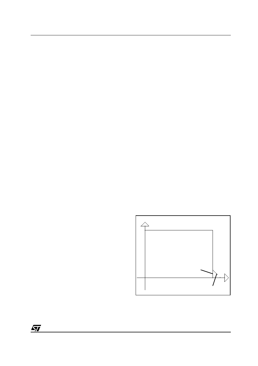
The relation between the controlled current and
the controlled output voltage can be described
with a square characteristic as shown in the
following V/I output-power graph.
Fig. 3: Output voltage versus output current
R
1
R
2
V
ref
V
out
V
ref
–
---------------------------
=
R
sense
I
lim
V
sense
=
V
sense
R
5
V
ref
R
4
R
5
+
--------------------
=
I
lim
R
5
V
ref
R
4
R
5
+
() R
sense
------------------------------------------------
=
P
lim
V
se nse Ilim
=
Vout
Iout
Voltage regulation
C
u
rr
ent
r
egulation
TSM1011 Vcc : independent power supply
0
Secondary current regulation
TSM1011 Vcc : On power output
Primary current regulation
相关PDF资料 |
PDF描述 |
|---|---|
| TSM1012IDT | 1-CHANNEL POWER SUPPLY SUPPORT CKT, PDSO8 |
| TSM1012IST | 1-CHANNEL POWER SUPPLY SUPPORT CKT, PDSO8 |
| TSM1012AIDT | 1-CHANNEL POWER SUPPLY SUPPORT CKT, PDSO8 |
| TSM1013IST | 1-CHANNEL POWER SUPPLY SUPPORT CKT, PDSO8 |
| TSM1013AIDT | 1-CHANNEL POWER SUPPLY SUPPORT CKT, PDSO8 |
相关代理商/技术参数 |
参数描述 |
|---|---|
| TSM1011IDT | 功能描述:电池管理 Constant Vltg Current Controller RoHS:否 制造商:Texas Instruments 电池类型:Li-Ion 输出电压:5 V 输出电流:4.5 A 工作电源电压:3.9 V to 17 V 最大工作温度:+ 85 C 最小工作温度:- 40 C 封装 / 箱体:VQFN-24 封装:Reel |
| TSM1011IS | 制造商:STMICROELECTRONICS 制造商全称:STMicroelectronics 功能描述:Constant Voltage and Constant Current Controller for Battery Chargers and Adapters |
| TSM1011IST | 功能描述:电池管理 Constant Vltg Current Controller RoHS:否 制造商:Texas Instruments 电池类型:Li-Ion 输出电压:5 V 输出电流:4.5 A 工作电源电压:3.9 V to 17 V 最大工作温度:+ 85 C 最小工作温度:- 40 C 封装 / 箱体:VQFN-24 封装:Reel |
| TSM1012 | 制造商:STMICROELECTRONICS 制造商全称:STMicroelectronics 功能描述:LOW CONSUMPTION VOLTAGE AND CURRENT CONTROLLER FOR BATTERY CHARGERS AND ADAPTORS |
| TSM1012AI | 制造商:STMICROELECTRONICS 制造商全称:STMicroelectronics 功能描述:LOW CONSUMPTION VOLTAGE AND CURRENT CONTROLLER FOR BATTERY CHARGERS AND ADAPTORS |
发布紧急采购,3分钟左右您将得到回复。