- 您现在的位置:买卖IC网 > PDF目录297617 > TSPC603PVGU8ME 32-BIT, 200 MHz, RISC PROCESSOR, CBGA255 PDF资料下载
参数资料
| 型号: | TSPC603PVGU8ME |
| 元件分类: | 微控制器/微处理器 |
| 英文描述: | 32-BIT, 200 MHz, RISC PROCESSOR, CBGA255 |
| 封装: | CBGA-255 |
| 文件页数: | 3/38页 |
| 文件大小: | 704K |
| 代理商: | TSPC603PVGU8ME |
第1页第2页当前第3页第4页第5页第6页第7页第8页第9页第10页第11页第12页第13页第14页第15页第16页第17页第18页第19页第20页第21页第22页第23页第24页第25页第26页第27页第28页第29页第30页第31页第32页第33页第34页第35页第36页第37页第38页
TSPC603p
11/38
B. DETAILED SPECIFICATIONS
1. SCOPE
This drawing describes the specific requirements for the microprocessor TSPC603p, in compliance with MIL-STD-883 class B or
TCS standard screening.
2. APPLICABLE DOCUMENTS
1) MIL-STD-883 : Test methods and procedures for electronics.
2) MIL-PRF-38535 appendix A : General specifications for microcircuits.
3. REQUIREMENTS
3.1. General
The microcircuits are in accordance with the applicable documents and as specified herein.
3.2. Design and construction
3.2.1. Terminal connections
Depending on the package, the terminal connections shall be is shown in Figure 2 and Figure 4 (§ A. GENERAL DESCRIPTION).
3.2.2. Lead material and finish
Lead material and finish shall be as specified in MIL-STD-1835 (see enclosed § 8)
3.2.3. Hermetic Package
The macrocircuits are packaged in 240 pin ceramic quad flat packages (see § 8.1)
The precise case outlines are described at the end of the specification (§ 8.1) and into MIL-STD-1835.
3.3. Absolute maximum ratings
Stresses above the absolute maximum rating may cause permanent damage to the device. Extended operation at the maximum
levels may degrade performance and affect reliability.
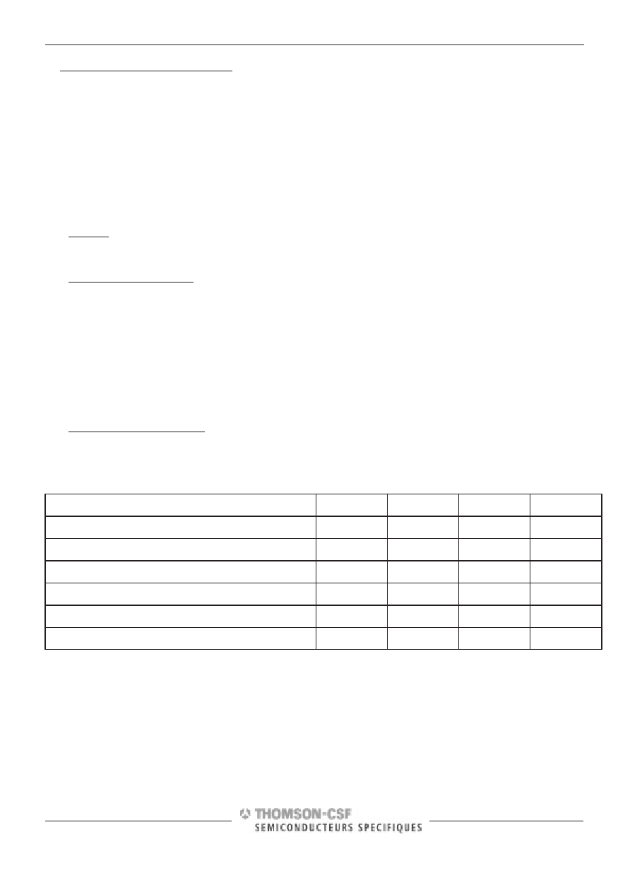
Table 5 : Absolute maximum rating for the 603p
Parameter
Symbol
Min
Max
Unit
Core supply voltage
Vdd
-0.3
2.75
V
PLL supply voltage
AVdd
-0.3
2.75
V
I/O supply voltage
OVdd
-0.3
3.6
V
Input voltage
Vin
-0.3
5.5
V
Storage temperature range
Tstg
-55
+150
°C
Operating temperature case
Tc
-55
+130
°C
Notes:
1. Functional operating conditions are given in AC and DC electrical specifications. Stresses beyond the absolute maximums listed may affect
device reliability or cause permanent damage to the device.
2. Caution : Input voltage must not be greater than the OVdd supply voltage by more than 2.5 V at all times including during power-on reset.
3. Caution : OVdd voltage must not be greater than Vdd/AVdd supply voltage by more than 1.2 V at all times including during power-on reset.
4. Caution : Vdd/AVdd voltage must not be greater than OVdd supply voltage by more than 0.4 V at all times including during power-on reset.
相关PDF资料 |
PDF描述 |
|---|---|
| TSPC603PVGU/T6ME | 32-BIT, 166 MHz, RISC PROCESSOR, CBGA255 |
| TSPC603PVG6ME | 32-BIT, 166 MHz, RISC PROCESSOR, CBGA255 |
| TSPC603PMGB/C8ME | 32-BIT, 200 MHz, RISC PROCESSOR, CBGA255 |
| TSPC603PMGB/C6ME | 32-BIT, 166 MHz, RISC PROCESSOR, CBGA255 |
| TSPC603PMGB/C6LE | 32-BIT, 166 MHz, RISC PROCESSOR, CBGA255 |
相关代理商/技术参数 |
参数描述 |
|---|---|
| TSPC603R | 制造商:ATMEL 制造商全称:ATMEL Corporation 功能描述:PowerPC 603e RISC Microprocessor Family PID7t-603e |
| TSPC603RCAB/Q8L | 制造商:ATMEL 制造商全称:ATMEL Corporation 功能描述:PowerPC 603e RISC Microprocessor Family PID7t-603e |
| TSPC603RCAB/Q8LC | 制造商:ATMEL 制造商全称:ATMEL Corporation 功能描述:PowerPC 603e RISC Microprocessor Family PID7t-603e |
| TSPC603RMAB/Q8L | 制造商:ATMEL 制造商全称:ATMEL Corporation 功能描述:PowerPC 603e RISC Microprocessor Family PID7t-603e |
| TSPC603RMAB/Q8LC | 制造商:ATMEL 制造商全称:ATMEL Corporation 功能描述:PowerPC 603e RISC Microprocessor Family PID7t-603e |
发布紧急采购,3分钟左右您将得到回复。