- 您现在的位置:买卖IC网 > PDF目录15080 > UC3844NG (ON Semiconductor)IC REG CTRLR PWM CM 8-DIP PDF资料下载
参数资料
| 型号: | UC3844NG |
| 厂商: | ON Semiconductor |
| 文件页数: | 9/16页 |
| 文件大小: | 0K |
| 描述: | IC REG CTRLR PWM CM 8-DIP |
| 产品变化通告: | Product Discontinuation 15/May/2006 |
| 标准包装: | 50 |
| PWM 型: | 电流模式 |
| 输出数: | 1 |
| 频率 - 最大: | 60kHz |
| 占空比: | 50% |
| 电源电压: | 10 V ~ 30 V |
| 降压: | 无 |
| 升压: | 是 |
| 回扫: | 是 |
| 反相: | 是 |
| 倍增器: | 无 |
| 除法器: | 无 |
| Cuk: | 无 |
| 隔离: | 是 |
| 工作温度: | 0°C ~ 70°C |
| 封装/外壳: | 8-DIP(0.300",7.62mm) |
| 包装: | 管件 |
| 其它名称: | UC3844NGOS |
�� �
�
�UC3844,� UC3845,� UC2844,� UC2845�
�Undervoltage� Lockout�
�Two� undervoltage� lockout� comparators� have� been�
�incorporated� to� guarantee� that� the� IC� is� fully� functional�
�before� the� output� stage� is� enabled.� The� positive� power�
�supply� terminal� (V� CC� and� the� reference� output� (V� ref� )� are�
�each� monitored� by� separate� comparators.� Each� has� built� ?� in�
�hysteresis� to� prevent� erratic� output� behavior� as� their�
�respective� thresholds� are� crossed.� The� V� CC� comparator�
�upper� and� lower� thresholds� are� 16� V/10� V� for� the� UCX844,�
�and� 8.4� V/7.6� V� for� the� UCX845.� The� V� ref� comparator� upper�
�and� lower� thresholds� are� 3.6� V/3/4� V.� The� large� hysteresis�
�and� low� startup� current� of� the� UCX844� makes� it� ideally�
�suited� in� off� ?� line� converter� applications� where� efficient�
�bootstrap� startup� techniques� later� required� (Figure� 30).� The�
�UCX845� is� intended� for� lower� voltage� DC� ?� to� ?� DC� converter�
�applications.� A� 36� V� zener� is� connected� as� a� shunt� regulator�
�from� V� CC� to� ground.� Its� purpose� is� to� protect� the� IC� from�
�excessive� voltage� that� can� occur� during� system� startup.� The�
�minimum� operating� voltage� for� the� UCX844� is� 11� V� and�
�8.2� V� for� the� UCX845.�
�Output�
�These� devices� contain� a� single� totem� pole� output� stage� that�
�was� specifically� designed� for� direct� drive� of� power�
�MOSFETs.� It� is� capable� of� up� to� ±� 1.0� A� peak� drive� current�
�and� has� a� typical� rise� and� fall� time� of� 50� ns� with� a� 1.0� nF� load.�
�Additional� internal� circuitry� has� been� added� to� keep� the�
�Output� in� a� sinking� mode� whenever� and� undervoltage�
�lockout� is� active.� This� characteristic� eliminates� the� need� for�
�an� external� pull� ?� down� resistor.�
�The� SOIC� ?� 14� surface� mount� package� provides� separate�
�pins� for� V� C� (output� supply)� and� Power� Ground.� Proper�
�implementation� will� significantly� reduce� the� level� of�
�switching� transient� noise� imposed� on� the� control� circuitry.�
�This� becomes� particularly� useful� when� reducing� the� I� pk(max)�
�clamp� level.� The� separate� V� C� supply� input� allows� the�
�V� ref�
�designer� added� flexibility� in� tailoring� the� drive� voltage�
�independent� of� V� CC.� A� zener� clamp� is� typically� connected�
�to� this� input� when� driving� power� MOSFETs� in� systems�
�where� V� CC� is� greater� the� 20� V.� Figure� 23� shows� proper�
�power� and� control� ground� connections� in� a� current� sensing�
�power� MOSFET� application.�
�Reference�
�The� 5.0� V� bandgap� reference� is� trimmed� to� ±� 1.0%�
�tolerance� at� T� J� =� 25� °� C� on� the� UC284X,� and� ±� 2.0%� on� the�
�UC384X.� Its� primary� purpose� is� to� supply� charging� current�
�to� the� oscillator� timing� capacitor.� The� reference� has� short�
�circuit� protection� and� is� capable� of� providing� in� excess� of�
�20� mA� for� powering� additional� control� system� circuitry.�
�Design� Considerations�
�Do� not� attempt� to� construct� the� converter� on�
�wire� ?� wrap� or� plug� ?� in� prototype� boards.� High� frequency�
�circuit� layout� techniques� are� imperative� to� prevent�
�pulsewidth� jitter.� This� is� usually� caused� by� excessive� noise�
�pick� ?� up� imposed� on� the� Current� Sense� or� Voltage� Feedback�
�inputs.� Noise� immunity� can� be� improved� by� lowering� circuit�
�impedances� at� these� points.� The� printed� circuit� layout� should�
�contain� a� ground� plane� with� low� ?� current� signal� and�
�high� ?� current� switch� and� output� grounds� returning� on�
�separate� paths� back� to� the� input� filter� capacitor.� Ceramic�
�bypass� capacitors� (0.1� m� F)� connected� directly� to� V� CC� ,� V� C� ,�
�and� V� ref� may� be� required� depending� upon� circuit� layout.�
�This� provides� a� low� impedance� path� for� filtering� the� high�
�frequency� noise.� All� high� current� loops� should� be� kept� as�
�short� as� possible� using� heavy� copper� runs� to� minimize�
�radiated� EMI.� The� Error� Amp� compensation� circuitry� and�
�the� converter� output� voltage� divider� should� be� located� close�
�to� the� IC� and� as� far� as� possible� from� the� power� switch� and�
�other� noise� generating� components.�
�8(14)�
�R�
�S�
�External�
�Sync�
�Input�
�0.01�
�R� T�
�C� T�
�47�
�4(7)�
�2(3)�
�+�
�?�
�R�
�EA�
�+�
�Bias�
�OSC�
�2R�
�R�
�R� A�
�R� B�
�6�
�5�
�2�
�C�
�8� 4�
�5.0k�
�+�
�?� R�
�Q�
�+�
�?�
�5.0k� MC1455�
�3�
�7�
�8(14)�
�4(7)�
�2(3)�
�+�
�?�
�R�
�R�
�EA�
�+�
�Bias�
�OSC�
�2R�
�R�
�1(1)�
�5(9)�
�1�
�1(1)�
�To�
�5(9)�
�The� diode� clamp� is� required� if� the� Sync� amplitude� is� large� enough� to�
�cause� the� bottom� side� of� CT� to� go� more� than� 300� mV� below� ground.�
�f=�
�1.44�
�(R� A� +� 2R� B� )C�
�D� max� =�
�R� B�
�R� A� +� 2R� B�
�Additional�
�UCX84XA’s�
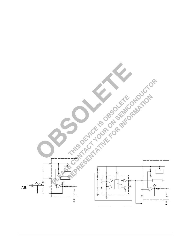
�Figure� 18.� External� Clock� Synchronization�
�Figure� 19.� External� Duty� Cycle� Clamp� and�
�Multi� ?� Unit� Synchronization�
�http://onsemi.com�
�9�
�相关PDF资料 |
PDF描述 |
|---|---|
| GBE50DHRT | CONN CARD EXTEND 100POS 1MM SLD |
| UC3843ADR2G | IC REG CTRLR FLYBK ISO CM 14SOIC |
| GSM08DTAT-S664 | CONN EDGECARD 16POS R/A .156 SLD |
| UC3842ANG | IC REG CTRLR FLYBK ISO PWM 8-DIP |
| UC3842ADR2G | IC REG CTRLR FLYBK ISO CM 14SOIC |
相关代理商/技术参数 |
参数描述 |
|---|---|
| UC3844NG4 | 功能描述:电流型 PWM 控制器 Current-Mode PWM Controller RoHS:否 制造商:Texas Instruments 开关频率:27 KHz 上升时间: 下降时间: 工作电源电压:6 V to 15 V 工作电源电流:1.5 mA 输出端数量:1 最大工作温度:+ 105 C 安装风格:SMD/SMT 封装 / 箱体:TSSOP-14 |
| UC3844P | 制造商:Texas Instruments 功能描述: |
| UC3844Q | 制造商:未知厂家 制造商全称:未知厂家 功能描述:Current-Mode SMPS Controller |
| UC3844QTR | 制造商:未知厂家 制造商全称:未知厂家 功能描述:Current-Mode SMPS Controller |
| UC3844-S08-R | 制造商:UTC-IC 制造商全称:UTC-IC 功能描述:HIGH PERFORMANCE CURRENT MODE PWM CONTROLLERS |
发布紧急采购,3分钟左右您将得到回复。