- 您现在的位置:买卖IC网 > PDF目录20300 > UCC28050D (Texas Instruments)IC PFC CTRLR TRANSITION 8SOIC PDF资料下载
参数资料
| 型号: | UCC28050D |
| 厂商: | Texas Instruments |
| 文件页数: | 6/32页 |
| 文件大小: | 0K |
| 描述: | IC PFC CTRLR TRANSITION 8SOIC |
| 标准包装: | 75 |
| 模式: | 间歇(跃迁) |
| 频率 - 开关: | 200kHz |
| 电流 - 启动: | 75µA |
| 电源电压: | 15.4 V ~ 18 V |
| 工作温度: | -40°C ~ 105°C |
| 安装类型: | 表面贴装 |
| 封装/外壳: | 8-SOIC(0.154",3.90mm 宽) |
| 供应商设备封装: | 8-SOIC |
| 包装: | 管件 |
| 产品目录页面: | 1052 (CN2011-ZH PDF) |
| 配用: | 296-19044-ND - EVAL MODULE FOR UCC38050 296-19036-ND - EVAL MODULE FOR UCC28051 |
| 其它名称: | 296-13708-5 |
第1页第2页第3页第4页第5页当前第6页第7页第8页第9页第10页第11页第12页第13页第14页第15页第16页第17页第18页第19页第20页第21页第22页第23页第24页第25页第26页第27页第28页第29页第30页第31页第32页
�� �
�
�UCC28050,� UCC28051�
�UCC38050,� UCC38051�
�SLUS515F?SEPTEMBER� 2002� ?� REVISED� MARCH� 2009�
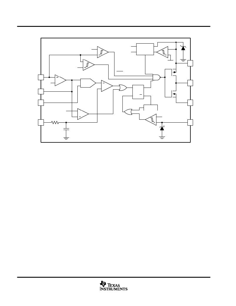
�BLOCK� DIAGRAM�
�2.7/2.5� V�
�+�
�OVP�
�VREF�
�INT.� BIAS�
�VREFAND�
�BIAS� REG�
�UVLO�
�+�
�0.67/0.57� V�
�0.23/0.15� V�
�+�
�ENABLE�
�VREF�
�GOOD�
�REF�
�8�
�VCC�
�V0_SNS�
�1�
�gm� VOL.�
�ERROR� AMP�
�OVP�
�COMP�
�2�
�2.5� V�
�+�
�x�
�x� MULT�
�PWM�
�+�
�R�
�Q�
�7�
�DRV�
�S�
�Q�
�MULTIN�
�3�
�ZERO�
�POWER�
�6�
�GND�
�DETECT�
�TIMER�
�2.3� V�
�+�
�40� k� W�
�+�
�1.7/1.4� V�
�CS�
�4�
�5�
�ZCD�
�5� pF�
�UDG?02008�
�PIN� DESCRIPTIONS�
�VO_SNS� (Pin� 1):� This� pin� senses� the� boost� regulator� output� voltage� through� a� voltage� divider.� Internally,� this�
�pin� is� the� inverting� input� to� the� transconductance� amplifier� (with� a� nominal� value� of� 2.5� V)� and� also� is� input� to�
�the� OVP� comparator.� Additionally,� pulling� this� pin� below� the� ENABLE� threshold� turns� off� the� output� switching,�
�ensuring� that� the� gate� drive� is� held� off� while� the� boost� output� is� pre-charging� and� also� ensuring� no� runaway� if�
�feedback� path� is� open.�
�COMP� (Pin� 2):� Output� of� the� transconductance� error� amplifier.� Loop� compensation� components� are� connected�
�between� this� pin� and� ground.� The� output� current� capability� of� this� pin� is� 10-� μ� A� under� normal� conditions,� but�
�increases� to� about� 1-mA� when� the� differential� input� is� greater� than� the� specified� values� in� the� specifications�
�table.� This� voltage� is� one� of� the� inputs� to� the� multiplier,� with� a� dynamic� input� range� of� 2.5� V� to� 3.8� V.� During� zero�
�power� or� overvoltage� conditions,� this� pin� goes� below� 2.5� V� nominal.� When� it� goes� below� 2.3� V,� the� zero� power�
�comparator� is� activated� which� prevents� the� gate� drive� from� switching.�
�MULTIN� (Pin� 3):� This� pin� senses� the� instantaneous� boost� regulator� input� voltage� through� a� voltage� divider.� The�
�voltage� acts� as� one� of� the� inputs� to� the� internal� multiplier.� Recommended� operating� range� is� 0� V� to� 2.5� V� at� high�
�line.�
�PIN� DESCRIPTIONS� (continued)�
�CS� (Pin� 4):� This� pin� senses� the� instantaneous� switch� current� in� the� boost� switch� and� uses� it� as� the� internal� ramp�
�for� PWM� comparator.� The� internal� circuitry� filters� out� switching� noise� spikes� without� requiring� external�
�components.� In� addition,� an� external� R-C� filter� may� be� required� to� suppress� the� noise� spikes.� An� internal� clamp�
�on� the� multiplier� output� terminates� the� switching� cycle� if� this� pin� voltage� exceeds� 1.7� V.� Additional� external�
�filtering� may� be� required.� CS� threshold� is� approximately� equal� to:�
�6�
�www.ti.com�
�相关PDF资料 |
PDF描述 |
|---|---|
| HBM12DRUS | CONN EDGECARD 24POS .156 DIP SLD |
| V110A24C300BF3 | CONVERTER MOD DC/DC 24V 300W |
| ACM28DRMN | CONN EDGECARD 56POS .156 WW |
| T95R226M050HZSS | CAP TANT 22UF 50V 20% 2824 |
| VI-J22-CX-F1 | CONVERTER MOD DC/DC 15V 75W |
相关代理商/技术参数 |
参数描述 |
|---|---|
| UCC28050DG4 | 功能描述:功率因数校正 IC Transition Mode PFC Cntrlr RoHS:否 制造商:Fairchild Semiconductor 开关频率:300 KHz 最大功率耗散: 最大工作温度:+ 125 C 安装风格:SMD/SMT 封装 / 箱体:SOIC-8 封装:Reel |
| UCC28050DR | 功能描述:功率因数校正 IC Transition Mode PFC Controller RoHS:否 制造商:Fairchild Semiconductor 开关频率:300 KHz 最大功率耗散: 最大工作温度:+ 125 C 安装风格:SMD/SMT 封装 / 箱体:SOIC-8 封装:Reel |
| UCC28050DRG4 | 功能描述:功率因数校正 IC Transition Mode PFC Controller RoHS:否 制造商:Fairchild Semiconductor 开关频率:300 KHz 最大功率耗散: 最大工作温度:+ 125 C 安装风格:SMD/SMT 封装 / 箱体:SOIC-8 封装:Reel |
| UCC28050P | 功能描述:功率因数校正 IC Transition Mode PFC Controller RoHS:否 制造商:Fairchild Semiconductor 开关频率:300 KHz 最大功率耗散: 最大工作温度:+ 125 C 安装风格:SMD/SMT 封装 / 箱体:SOIC-8 封装:Reel |
| UCC28050PE4 | 功能描述:功率因数校正 IC Transition Mode PFC Controller RoHS:否 制造商:Fairchild Semiconductor 开关频率:300 KHz 最大功率耗散: 最大工作温度:+ 125 C 安装风格:SMD/SMT 封装 / 箱体:SOIC-8 封装:Reel |
发布紧急采购,3分钟左右您将得到回复。