- 您现在的位置:买卖IC网 > PDF目录245264 > UPD121A10T1F-E1-AT 1 V FIXED POSITIVE REGULATOR, PSSO4 PDF资料下载
参数资料
| 型号: | UPD121A10T1F-E1-AT |
| 元件分类: | 固定正电压单路输出标准稳压器 |
| 英文描述: | 1 V FIXED POSITIVE REGULATOR, PSSO4 |
| 封装: | LEAD FREE, TO-252, MP-3ZK, 6 PIN |
| 文件页数: | 1/10页 |
| 文件大小: | 208K |
| 代理商: | UPD121A10T1F-E1-AT |
The information in this document is subject to change without notice. Before using this document, please
confirm that this is the latest version.
Not all products and/or types are available in every country. Please check with an NEC Electronics
sales representative for availability and additional information.
2007
MOS INTEGRATED CIRCUIT
μ PD121A10
2-POWER SUPPLY INPUT METHOD
1.0 V/2.0 A REGULATOR
DATA SHEET
Document No. G18843EJ1V0DS00 (1st edition)
Date Published July 2007 NS
Printed in Japan
DESCRIPTION
μ PD121A10 is the CMOS regulator which can output 2.0 A current. This regulator is suitable for power supply for 1.0
V ASIC core, for example our companies’ CB-90 (90 nm process LSI) etc. The dropout voltage is made small (0.7 V
MAX. (IO = 1.0 A) by dividing bias voltage (VDD) from input voltage (VIN). Therefore this product can output under the
conditions, VIN
≥ 1.62 V (VDD ≥ 4.0 V). Output voltage can be adjustable between 0.95 and 1.15 V.
FEATURES
Output Current: 2.0 A
Output Voltage: 0.95 to 1.15 V
Bias Voltage: 4.0 to 5.5 V
Reference Voltage Tolerance: VREF ± 10 mV (TJ = 25°C)
Low Dropout Voltage: VDIF = 0.7 V MAX. (IO = 1.0 A)
On-chip over-current protection circuit
On-chip thermal shut down circuit
APPLICATIONS
This regulator is suitable for low power supply voltage IC,
for example core of CB-90 (90 nm process LSI) etc.
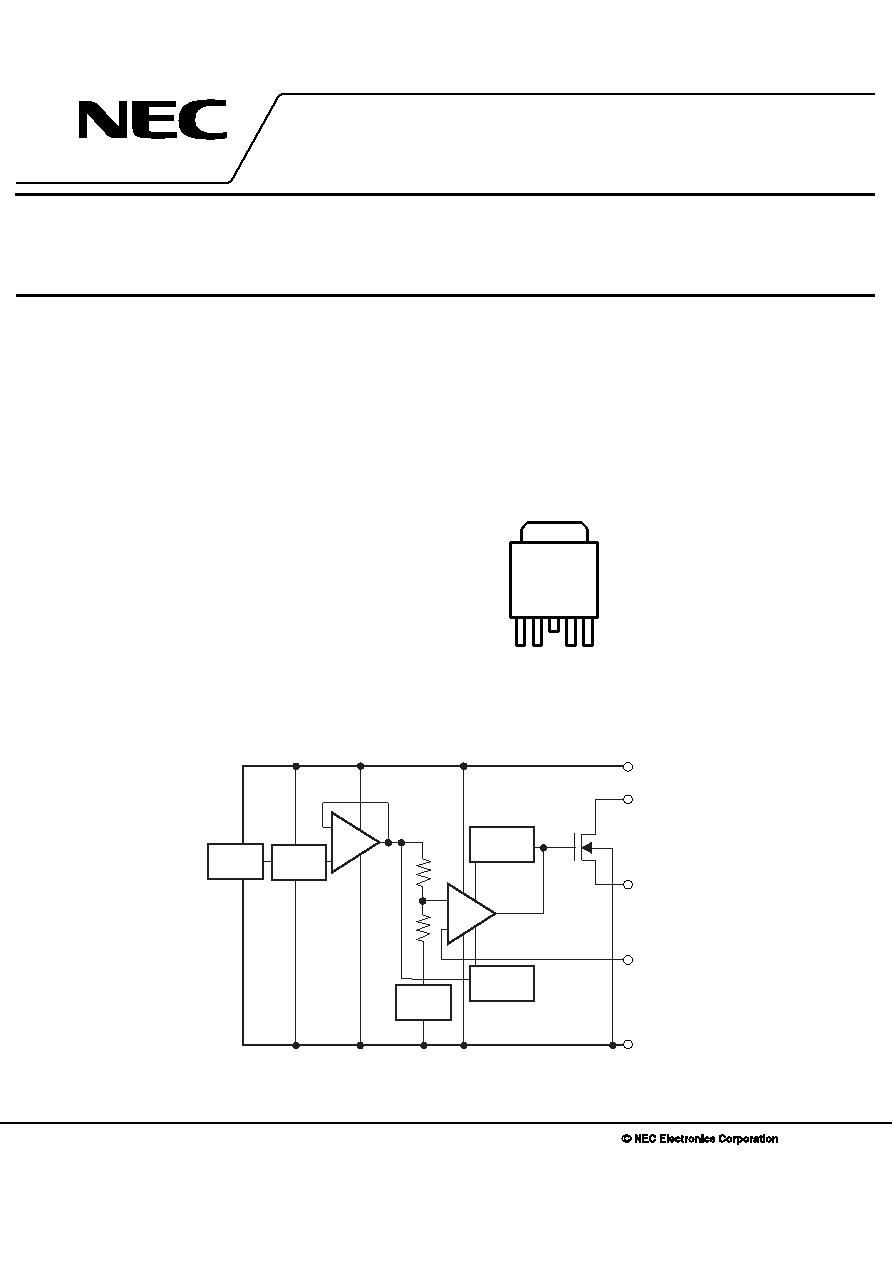
BLOCK DIAGRAM
+
VDD
INPUT
OUTPUT
SENSE
GND
Reference
voltage
Constant
current
Over-current
protection
Thermal
shut down
Error
amp.
Buffer
Triming
PIN CONFIGURATION (Marking Side)
5-PIN TO-252 (5-PIN MP-3ZK)
123 4 5
6
Note No.3 pin is cut and can not be connected to
substrate. No.6 is Fin and common to GND pin.
1. INPUT
2. VDD (ON/OFF)
3. GND
Note
4. SENSE
5. OUTPUT
6. GND (Fin)
相关PDF资料 |
PDF描述 |
|---|---|
| UPD121A10T1F-E2-AT | 1 V FIXED POSITIVE REGULATOR, PSSO4 |
| UPD121A10T1F | 1 V FIXED POSITIVE REGULATOR, PSSO4 |
| UPC317HF | 1.3 V-30 V ADJUSTABLE POSITIVE REGULATOR, PSFM3 |
| UPC78L15T-AZ | 15 V FIXED POSITIVE REGULATOR, PSSO3 |
| UPC78N05H-AZ | 5 V FIXED POSITIVE REGULATOR, PSIP3 |
相关代理商/技术参数 |
参数描述 |
|---|---|
| UPD121A10T1F-E2-AT | 制造商:NEC 制造商全称:NEC 功能描述:MOS INTEGRATED CIRCUIT |
| UPD121W00AT1F | 制造商:NEC 制造商全称:NEC 功能描述:MOS INTEGRATED CIRCUIT |
| UPD121W00AT1F-E1-AT | 制造商:NEC 制造商全称:NEC 功能描述:MOS INTEGRATED CIRCUIT |
| UPD121W00AT1F-E2-AT | 制造商:NEC 制造商全称:NEC 功能描述:MOS INTEGRATED CIRCUIT |
| UPD121W18AT1F | 制造商:NEC 制造商全称:NEC 功能描述:MOS INTEGRATED CIRCUIT |
发布紧急采购,3分钟左右您将得到回复。