- 您现在的位置:买卖IC网 > PDF目录378741 > UPD65808-QFP120P1.2SQ ASIC PDF资料下载
参数资料
| 型号: | UPD65808-QFP120P1.2SQ |
| 英文描述: | ASIC |
| 中文描述: | 专用集成电路 |
| 文件页数: | 17/64页 |
| 文件大小: | 399K |
| 代理商: | UPD65808-QFP120P1.2SQ |
第1页第2页第3页第4页第5页第6页第7页第8页第9页第10页第11页第12页第13页第14页第15页第16页当前第17页第18页第19页第20页第21页第22页第23页第24页第25页第26页第27页第28页第29页第30页第31页第32页第33页第34页第35页第36页第37页第38页第39页第40页第41页第42页第43页第44页第45页第46页第47页第48页第49页第50页第51页第52页第53页第54页第55页第56页第57页第58页第59页第60页第61页第62页第63页第64页
17
μ
PD64A, 65
Data Sheet U14380EJ2V0DS00
3.2.4 S
2
port (bit 1 of P1)
The S
2
port is an input port.
Use of the STOP mode release of the S
2
port can be specified by bit 3 of the P4 register.
When using the pin as a key input from a key matrix, enable (bit 3 of P4 register is set to 1) the use of the STOP
mode release (at this time, a pull-down resistor is connected internally.) When the STOP mode release is disabled
(bit 3 of P4 register is set to 0), it can be used as the input port which does not release the STOP mode even if
the release condition is established (at this time, a pull-down resistor is not connected internally.)
The state of the pin can be read in both cases.
At reset, the pin is set to INPUT mode where the STOP mode release is disabled, and goes to high-impedance
state.
3.3 Control Register 0 (P3)
Control register 0 consists of 8 bits. The contents that can be controlled are as shown below.
When reset, the register becomes 0000 0011B.
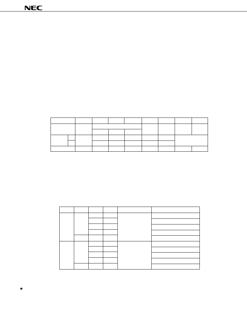
Table 3-4. Control Register 0 (P3)
Bit
b
7
b
6
b
5
b
4
b
3
b
2
b
1
b
0
Name
—
DP (Data pointer)
DP
10
Note
DP
9
TCTL
CARY
MOD
1
MOD
0
DP
8
Set
0
Fixed
0
0
0
1/1
ON
Refer to
Table 3-5
.
value
1
to “0”
1
1
1
1/2
OFF
When reset0
0
0
0
0
0
0
1
1
b
0
, b
1
: These bits specify the carrier frequency and duty ratio of the REM output.
b
2
: This bit specifies the availability of the carrier of the frequency specified by b
0
and b
1
.
“0” = ON (with carrier); “1” = OFF (without carrier; high level)
b
3
: This bit changes the carrier frequency and the timer clock’s frequency division ratio.
“0” = 1/1 (carrier frequency: the specified value of b
0
and b
1
; timer clock: f
X
/64)
“1” = 1/2 (carrier frequency: half of the specified value of b
0
and b
1
; timer clock: f
X
/128)
Table 3-5. Timer Clock and Carrier Frequency Setup
b
3
b
2
b
1
b
0
Timer Clock
Carrier Frequency (Duty Ratio)
0
0
0
0
f
X
/64
f
X
/8 (Duty 1/2)
0
1
f
X
/64 (Duty 1/2)
1
0
f
X
/96 (Duty 1/2)
1
1
f
X
/96 (Duty 1/3)
1
×
×
Without carrier (high level)
0
0
0
0
f
X
/128
f
X
/16 (Duty 1/2)
0
1
f
X
/128 (Duty 1/2)
1
0
f
X
/192 (Duty 1/2)
1
1
f
X
/192 (Duty 1/3)
1
×
×
Without carrier (high level)
b
4
, b
5
, b
6
: These bits specify the high-order 3 bits (DP
8
, DP
9
and DP
10
) of ROM’s data pointer.
Note
Set DP
10
of the
μ
PD64A to "0".
Remark
×
: don’t care
相关PDF资料 |
PDF描述 |
|---|---|
| UPD65808-QFP160P1.2SQ | ASIC |
| UPD65810 | ASIC |
| UPD65810-QFP100P.63SQ | ASIC |
| UPD65810-QFP100P.7X.9 | ASIC |
| UPD65810-QFP120P.63SQ | ASIC |
相关代理商/技术参数 |
参数描述 |
|---|---|
| UPD65808-QFP160P1.2SQ | 制造商:未知厂家 制造商全称:未知厂家 功能描述:ASIC |
| UPD65810 | 制造商:未知厂家 制造商全称:未知厂家 功能描述:ASIC |
| UPD65810-QFP100P.63SQ | 制造商:未知厂家 制造商全称:未知厂家 功能描述:ASIC |
| UPD65810-QFP100P.7X.9 | 制造商:未知厂家 制造商全称:未知厂家 功能描述:ASIC |
| UPD65810-QFP120P.63SQ | 制造商:未知厂家 制造商全称:未知厂家 功能描述:ASIC |
发布紧急采购,3分钟左右您将得到回复。