- 您现在的位置:买卖IC网 > PDF目录200646 > UPD78F0397GC(T2)-8EU-A 8-BIT, FLASH, 20 MHz, MICROCONTROLLER, PQFP100 PDF资料下载
参数资料
| 型号: | UPD78F0397GC(T2)-8EU-A |
| 元件分类: | 微控制器/微处理器 |
| 英文描述: | 8-BIT, FLASH, 20 MHz, MICROCONTROLLER, PQFP100 |
| 封装: | 14 X 14 MM, LEAD FREE, FINE PITCH, PLASTIC, LQFP-100 |
| 文件页数: | 173/321页 |
| 文件大小: | 4156K |
| 代理商: | UPD78F0397GC(T2)-8EU-A |
第1页第2页第3页第4页第5页第6页第7页第8页第9页第10页第11页第12页第13页第14页第15页第16页第17页第18页第19页第20页第21页第22页第23页第24页第25页第26页第27页第28页第29页第30页第31页第32页第33页第34页第35页第36页第37页第38页第39页第40页第41页第42页第43页第44页第45页第46页第47页第48页第49页第50页第51页第52页第53页第54页第55页第56页第57页第58页第59页第60页第61页第62页第63页第64页第65页第66页第67页第68页第69页第70页第71页第72页第73页第74页第75页第76页第77页第78页第79页第80页第81页第82页第83页第84页第85页第86页第87页第88页第89页第90页第91页第92页第93页第94页第95页第96页第97页第98页第99页第100页第101页第102页第103页第104页第105页第106页第107页第108页第109页第110页第111页第112页第113页第114页第115页第116页第117页第118页第119页第120页第121页第122页第123页第124页第125页第126页第127页第128页第129页第130页第131页第132页第133页第134页第135页第136页第137页第138页第139页第140页第141页第142页第143页第144页第145页第146页第147页第148页第149页第150页第151页第152页第153页第154页第155页第156页第157页第158页第159页第160页第161页第162页第163页第164页第165页第166页第167页第168页第169页第170页第171页第172页当前第173页第174页第175页第176页第177页第178页第179页第180页第181页第182页第183页第184页第185页第186页第187页第188页第189页第190页第191页第192页第193页第194页第195页第196页第197页第198页第199页第200页第201页第202页第203页第204页第205页第206页第207页第208页第209页第210页第211页第212页第213页第214页第215页第216页第217页第218页第219页第220页第221页第222页第223页第224页第225页第226页第227页第228页第229页第230页第231页第232页第233页第234页第235页第236页第237页第238页第239页第240页第241页第242页第243页第244页第245页第246页第247页第248页第249页第250页第251页第252页第253页第254页第255页第256页第257页第258页第259页第260页第261页第262页第263页第264页第265页第266页第267页第268页第269页第270页第271页第272页第273页第274页第275页第276页第277页第278页第279页第280页第281页第282页第283页第284页第285页第286页第287页第288页第289页第290页第291页第292页第293页第294页第295页第296页第297页第298页第299页第300页第301页第302页第303页第304页第305页第306页第307页第308页第309页第310页第311页第312页第313页第314页第315页第316页第317页第318页第319页第320页第321页
CHAPTER 13 LCD CONTROLLER/DRIVER
254
User’s Manual U15075EJ1V0UM00
13.6 Common and Segment Signals
Each pixel of the LCD panel turns on when the potential difference between the corresponding common and
segment signals becomes higher than a specific voltage (LCD drive voltage, VLCD). It turns off when the potential
difference becomes lower than VLCD.
Applying DC voltage to the common and segment signals for an LCD panel would deteriorate it. To avoid this
problem, this LCD panel is driven with AC voltage.
(1)
Common signals
Each common signal is selected sequentially according to a specified number of time slots at the timing
listed in Table 13-4. In the static display mode, the same signal is output to COM0 to COM3 in common.
In the three-time slot mode, keep the COM3 pin open.
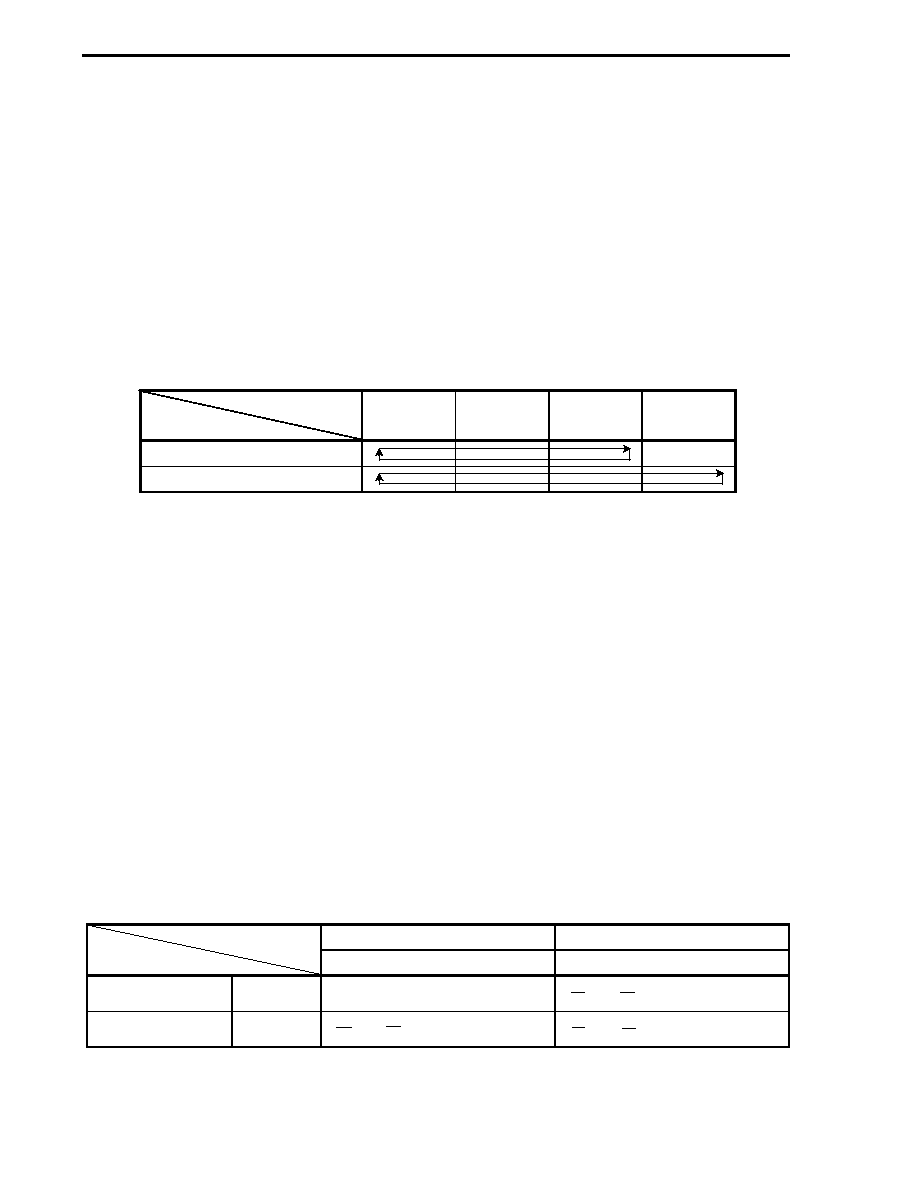
Table 13-4. COM Signals
COM Signal
Number of Time Slots
COM0
COM1
COM2
COM3
Three-time slot mode
Open
Four-time slot mode
(2)
Segment signals
The segment signals correspond to LCD display data memory. Bits 0, 1, 2, and 3 of each byte are read in
synchronization with COM0, COM1, COM2, and COM3, respectively. If the contents of each bit are 1, it is
converted to the select voltage, and if 0, it is converted to the deselect voltage. The conversion results are
output to the segment pins.
Check, with the information given above, what combination of the front-surface electrodes (corresponding to
the segment signals) and the rear-surface electrodes (corresponding to the common signals) forms display
patterns in the LCD display data memory, and write the bit data that corresponds to the desired display
pattern on a one-to-one basis.
Bit 3 of the LCD display data memory is not used for LCD display in the three-time slot mode. So this bit
can be used for purposes other than display.
LCD display data memory bits 4 to 7 are fixed to 0.
(3)
Output waveforms of common and segment signals
Voltages listed in Table 13-5 are output as common and segment signals.
When both common and segment signals are at the select voltage, a display-on voltage of
±VLCD is
obtained. The other combinations of the signals correspond to the display-off voltage.
Table 13-5. LCD Drive Voltage
Segment Signal
Select Signal Level
Deselect Signal Level
Common Signal
VSS0/VLC0
VLC1/VLC2
Select signal level
VLC0/VSS0
–VLCD/+VLCD
–
VLCD/+
VLCD
Deselect signal level
VLC2/VLC1
–
VLCD/+
VLCD
–
VLCD/+
VLCD
1
3
1
3
1
3
1
3
1
3
1
3
相关PDF资料 |
PDF描述 |
|---|---|
| UPD78F0397GC(R)-8EU-A | 8-BIT, FLASH, 20 MHz, MICROCONTROLLER, PQFP100 |
| UPD78F0397DGF(T)-JBT-A | 8-BIT, FLASH, 20 MHz, MICROCONTROLLER, PQFP100 |
| UPD78F0397DGC(T)-8EU-A | 8-BIT, FLASH, 20 MHz, MICROCONTROLLER, PQFP100 |
| UPD78F0534FC(T)-AA1-A | 8-BIT, FLASH, 20 MHz, MICROCONTROLLER, PBGA64 |
| UPD78F0535GC(S)-UBS-A | 8-BIT, FLASH, 20 MHz, MICROCONTROLLER, PQFP64 |
相关代理商/技术参数 |
参数描述 |
|---|---|
| UPD78F0400GA-GAM-AX | 功能描述:IC MCU 8BIT 8KB FLASH 48LQFP RoHS:是 类别:集成电路 (IC) >> 嵌入式 - 微控制器, 系列:78K0/Lx3 标准包装:300 系列:78K0R/Ix3 核心处理器:78K/0R 芯体尺寸:16-位 速度:40MHz 连通性:3 线 SIO,I²C,LIN,UART/USART 外围设备:DMA,LVD,POR,PWM,WDT 输入/输出数:27 程序存储器容量:16KB(16K x 8) 程序存储器类型:闪存 EEPROM 大小:- RAM 容量:1K x 8 电压 - 电源 (Vcc/Vdd):2.7 V ~ 5.5 V 数据转换器:A/D 8x10b 振荡器型:内部 工作温度:-40°C ~ 85°C 封装/外壳:38-SSOP 包装:托盘 |
| UPD78F0401GA-GAM-AX | 功能描述:MCU 8BIT 16K FLASH RoHS:是 类别:集成电路 (IC) >> 嵌入式 - 微控制器, 系列:78K0/Lx3 标准包装:300 系列:78K0R/Ix3 核心处理器:78K/0R 芯体尺寸:16-位 速度:40MHz 连通性:3 线 SIO,I²C,LIN,UART/USART 外围设备:DMA,LVD,POR,PWM,WDT 输入/输出数:27 程序存储器容量:16KB(16K x 8) 程序存储器类型:闪存 EEPROM 大小:- RAM 容量:1K x 8 电压 - 电源 (Vcc/Vdd):2.7 V ~ 5.5 V 数据转换器:A/D 8x10b 振荡器型:内部 工作温度:-40°C ~ 85°C 封装/外壳:38-SSOP 包装:托盘 |
| UPD78F0402GA-GAM-AX | 功能描述:MCU 8BIT 24K FLASH RoHS:是 类别:集成电路 (IC) >> 嵌入式 - 微控制器, 系列:78K0/Lx3 标准包装:300 系列:78K0R/Ix3 核心处理器:78K/0R 芯体尺寸:16-位 速度:40MHz 连通性:3 线 SIO,I²C,LIN,UART/USART 外围设备:DMA,LVD,POR,PWM,WDT 输入/输出数:27 程序存储器容量:16KB(16K x 8) 程序存储器类型:闪存 EEPROM 大小:- RAM 容量:1K x 8 电压 - 电源 (Vcc/Vdd):2.7 V ~ 5.5 V 数据转换器:A/D 8x10b 振荡器型:内部 工作温度:-40°C ~ 85°C 封装/外壳:38-SSOP 包装:托盘 |
| UPD78F0403GA-GAM-AX | 功能描述:MCU 8BIT 32K FLASH RoHS:是 类别:集成电路 (IC) >> 嵌入式 - 微控制器, 系列:78K0/Lx3 标准包装:300 系列:78K0R/Ix3 核心处理器:78K/0R 芯体尺寸:16-位 速度:40MHz 连通性:3 线 SIO,I²C,LIN,UART/USART 外围设备:DMA,LVD,POR,PWM,WDT 输入/输出数:27 程序存储器容量:16KB(16K x 8) 程序存储器类型:闪存 EEPROM 大小:- RAM 容量:1K x 8 电压 - 电源 (Vcc/Vdd):2.7 V ~ 5.5 V 数据转换器:A/D 8x10b 振荡器型:内部 工作温度:-40°C ~ 85°C 封装/外壳:38-SSOP 包装:托盘 |
| UPD78F0410GA-GAM-AX | 功能描述:MCU 8BIT 8K FLASH RoHS:是 类别:集成电路 (IC) >> 嵌入式 - 微控制器, 系列:78K0/Lx3 标准包装:300 系列:78K0R/Ix3 核心处理器:78K/0R 芯体尺寸:16-位 速度:40MHz 连通性:3 线 SIO,I²C,LIN,UART/USART 外围设备:DMA,LVD,POR,PWM,WDT 输入/输出数:27 程序存储器容量:16KB(16K x 8) 程序存储器类型:闪存 EEPROM 大小:- RAM 容量:1K x 8 电压 - 电源 (Vcc/Vdd):2.7 V ~ 5.5 V 数据转换器:A/D 8x10b 振荡器型:内部 工作温度:-40°C ~ 85°C 封装/外壳:38-SSOP 包装:托盘 |
发布紧急采购,3分钟左右您将得到回复。