- 您现在的位置:买卖IC网 > PDF目录202172 > V54C3256164VAT6 (MOSEL-VITELIC) 16M X 16 SYNCHRONOUS DRAM, 5.4 ns, PDSO54 PDF资料下载
参数资料
| 型号: | V54C3256164VAT6 |
| 厂商: | MOSEL-VITELIC |
| 元件分类: | DRAM |
| 英文描述: | 16M X 16 SYNCHRONOUS DRAM, 5.4 ns, PDSO54 |
| 封装: | 0.400 INCH, PLASTIC, TSOP2-54 |
| 文件页数: | 7/52页 |
| 文件大小: | 853K |
| 代理商: | V54C3256164VAT6 |
第1页第2页第3页第4页第5页第6页当前第7页第8页第9页第10页第11页第12页第13页第14页第15页第16页第17页第18页第19页第20页第21页第22页第23页第24页第25页第26页第27页第28页第29页第30页第31页第32页第33页第34页第35页第36页第37页第38页第39页第40页第41页第42页第43页第44页第45页第46页第47页第48页第49页第50页第51页第52页
15
V54C3256(16/80/40)4V(T/S/B) Rev. 1.6 September 2002
MOSEL VITELIC
V54C3256(16/80/40)4V(T/S/B)
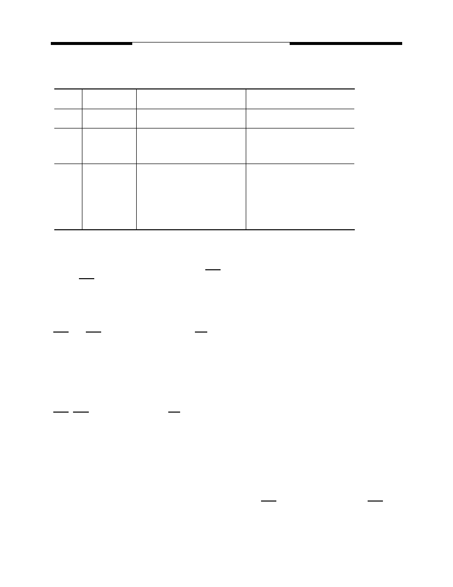
Burst Length and Sequence:
Refresh Mode
SDRAM has two refresh modes, Auto Refresh
and Self Refresh. Auto Refresh is similar to the CAS
-before-RAS refresh of conventional DRAMs. All of
banks must be precharged before applying any re-
fresh mode. An on-chip address counter increments
the word and the bank addresses and no bank infor-
mation is required for both refresh modes.
The chip enters the Auto Refresh mode, when
RAS and CAS are held low and CKE and WE are
held high at a clock timing. The mode restores word
line after the refresh and no external precharge
command is necessary. A minimum tRC time is re-
quired between two automatic refreshes in a burst
refresh mode. The same rule applies to any access
command after the automatic refresh operation.
The chip has an on-chip timer and the Self Re-
fresh mode is available. It enters the mode when
RAS, CAS, and CKE are low and WE is high at a
clock timing. All of external control signals including
the clock are disabled. Returning CKE to high en-
ables the clock and initiates the refresh exit opera-
tion. After the exit command, at least one tRC delay
is required prior to any access command.
DQM Function
DQM has two functions for data I/O read and
write operations. During reads, when it turns to
“high” at a clock timing, data outputs are disabled
and become high impedance after two clock delay
(DQM Data Disable Latency tDQZ ). It also provides
a data mask function for writes. When DQM is acti-
vated, the write operation at the next clock is prohib-
ited (DQM Write Mask Latency tDQW = zero clocks).
Power Down
In order to reduce standby power consumption, a
power down mode is available. All banks must be
precharged and the necessary Precharge delay
(trp) must occur before the SDRAM can enter the
Power Down mode. Once the Power Down mode is
initiated by holding CKE low, all of the receiver cir-
cuits except CLK and CKE are gated off. The Power
Down mode does not perform any refresh opera-
tions, therefore the device can’t remain in Power
Down mode longer than the Refresh period (tref) of
the device. Exit from this mode is performed by tak-
ing CKE “high”. One clock delay is required for
mode entry and exit.
Auto Precharge
Two
methods
are
available
to
precharge
SDRAMs. In an automatic precharge mode, the
CAS timing accepts one extra address, CA10, to
determine whether the chip restores or not after the
operation. If CA10 is high when a Read Command
is issued, the Read with Auto-Precharge function
is initiated. The SDRAM automatically enters the
precharge operation one clock before the last data
out for CAS latencies 2, two clocks for CAS laten-
cies 3 and three clocks for CAS latencies 4. If CA10
is high when a Write Command is issued, the Write
Burst
Length
Starting Address
(A2 A1 A0)
Sequential Burst Addressing
(decimal)
Interleave Burst Addressing
(decimal)
2
xx0
xx1
0, 1
1, 0
0, 1
1, 0
4x00
x01
x10
x11
0, 1, 2, 3
1, 2, 3, 0
2, 3, 0, 1
3, 0, 1, 2
0, 1, 2, 3
1, 0, 3, 2
2, 3, 0, 1
3, 2, 1, 0
8
000
001
010
011
100
101
110
111
0
1
2
3
4
5
6
7
1
2
3
4
5
6
7
0
2
3
4
5
6
7
0
1
3
4
5
6
7
0
1
2
4
5
6
7
0
1
2
3
5
6
7
0
1
2
3
4
6
7
0
1
2
3
4
5
7
0
1
2
3
4
5
6
0
1
2
3
4
5
6
7
1
0
3
2
5
4
7
6
2
3
0
1
6
7
4
5
3
2
1
0
7
6
5
4
5
6
7
0
1
2
3
5
4
7
6
1
0
3
2
6
7
4
5
2
3
0
1
7
6
5
4
3
2
1
0
相关PDF资料 |
PDF描述 |
|---|---|
| V54C3256404VDS8IPC | 64M X 4 SYNCHRONOUS DRAM, 6 ns, PBGA60 |
| V54C3256404VDUG7 | 64M X 4 SYNCHRONOUS DRAM, 5.4 ns, PBGA54 |
| V54C3256404VDLJ6 | 64M X 4 SYNCHRONOUS DRAM, 5.4 ns, PBGA60 |
| V54C3256404VDUI6 | 64M X 4 SYNCHRONOUS DRAM, 5.4 ns, PDSO54 |
| V54C3256404VDUS7 | 64M X 4 SYNCHRONOUS DRAM, 5.4 ns, PBGA60 |
相关代理商/技术参数 |
参数描述 |
|---|---|
| V54C3256164VB | 制造商:MOSEL 制造商全称:MOSEL 功能描述:256Mbit SDRAM 3.3 VOLT, TSOP II / SOC BGA / WBGA PACKAGE 16M X 16, 32M X 8, 64M X 4 |
| V54C3256164VBS | 制造商:MOSEL 制造商全称:MOSEL 功能描述:256Mbit SDRAM 3.3 VOLT, TSOP II / SOC BGA / WBGA PACKAGE 16M X 16, 32M X 8, 64M X 4 |
| V54C3256164VBT | 制造商:MOSEL 制造商全称:MOSEL 功能描述:256Mbit SDRAM 3.3 VOLT, TSOP II / SOC BGA / WBGA PACKAGE 16M X 16, 32M X 8, 64M X 4 |
| V54C3256164VBUC | 制造商:MOSEL 制造商全称:MOSEL 功能描述:LOW POWER 256Mbit SDRAM 3.3 VOLT, 54-BALL SOC BGA 54-PIN TSOPII 16M X 16 |
| V54C3256164VBUT | 制造商:MOSEL 制造商全称:MOSEL 功能描述:LOW POWER 256Mbit SDRAM 3.3 VOLT, 54-BALL SOC BGA 54-PIN TSOPII 16M X 16 |
发布紧急采购,3分钟左右您将得到回复。