- 您现在的位置:买卖IC网 > PDF目录202172 > V58C2256804SHUD6E (PROMOS TECHNOLOGIES INC) 32M X 8 DDR DRAM, PDSO66 PDF资料下载
参数资料
| 型号: | V58C2256804SHUD6E |
| 厂商: | PROMOS TECHNOLOGIES INC |
| 元件分类: | DRAM |
| 英文描述: | 32M X 8 DDR DRAM, PDSO66 |
| 封装: | 0.400 INCH, PLASTIC, MS-024FC, TSOP2-66 |
| 文件页数: | 4/60页 |
| 文件大小: | 1125K |
| 代理商: | V58C2256804SHUD6E |
第1页第2页第3页当前第4页第5页第6页第7页第8页第9页第10页第11页第12页第13页第14页第15页第16页第17页第18页第19页第20页第21页第22页第23页第24页第25页第26页第27页第28页第29页第30页第31页第32页第33页第34页第35页第36页第37页第38页第39页第40页第41页第42页第43页第44页第45页第46页第47页第48页第49页第50页第51页第52页第53页第54页第55页第56页第57页第58页第59页第60页
12
V58C2256(804/404/164)SH Rev. 1.1 July 2010
ProMOS TECHNOLOGIES
V58C2256(804/404/164)SH
Bank Activate Command
The Bank Activate command is issued by holding CAS and WE high with CS and RAS low at the rising
edge of the clock. The DDR SDRAM has four independent banks, so two Bank Select addresses (BA0 and
BA1) are supported. The Bank Activate command must be applied before any Read or Write operation can
be executed. The delay from the Bank Activate command to the first Read or Write command must meet or
exceed the minimum RAS to CAS delay time (tRCD min). Once a bank has been activated, it must be pre-
charged before another Bank Activate command can be applied to the same bank. The minimum time interval
between interleaved Bank Activate commands (Bank A to Bank B and vice versa) is the Bank to Bank delay
time (tRRD min).
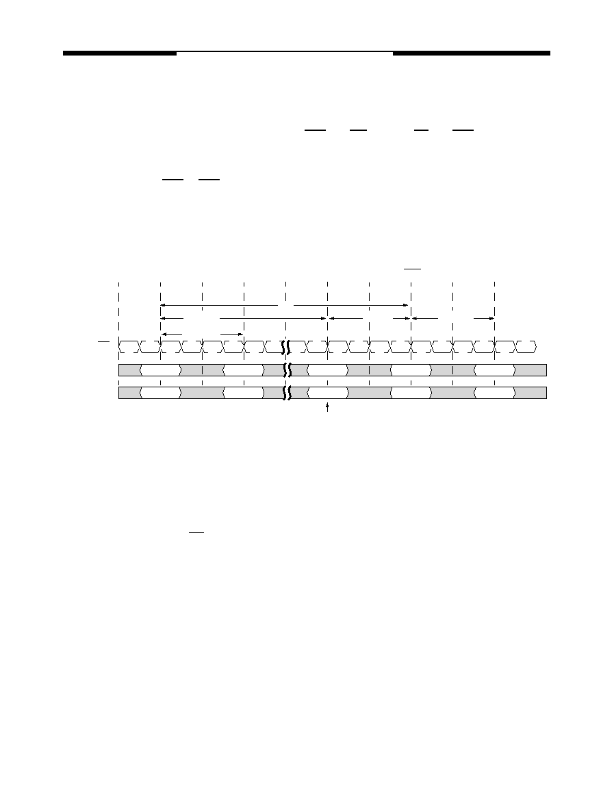
Bank Activation Timing
Read Operation
With the DLL enabled, all devices operating at the same frequency within a system are ensured to have
the same timing relationship between DQ and DQS relative to the CK input regardless of device density, pro-
cess variation, or technology generation.
The data strobe signal (DQS) is driven off chip simultaneously with the output data (DQ) during each read
cycle. The same internal clock phase is used to drive both the output data and data strobe signal off chip to
minimize skew between data strobe and output data. This internal clock phase is nominally aligned to the
input differential clock (CK, CK) by the on-chip DLL. Therefore, when the DLL is enabled and the clock fre-
quency is within the specified range for proper DLL operation, the data strobe (DQS), output data (DQ), and
the system clock (CK) are all nominally aligned.
Since the data strobe and output data are tightly coupled in the system, the data strobe signal may be de-
layed and used to latch the output data into the receiving device. The tolerance for skew between DQS and
DQ (tDQSQ) is tighter than that possible for CK to DQ (tAC) or DQS to CK (tDQSCK).
T0
T1
T2
T3
Tn
Tn+1
Tn+2
Tn+3
Tn+4
Tn+5
(CAS Latency = 2; Burst Length = Any)
tRRD(min)
tRP(min)
tRC
tRCD(min)
Begin Precharge Bank A
CK, CK
BA/Address
Command
Bank/Col
Read/A
Bank/Row
Activate/A
Activate/B
Pre/A
Bank/Row
Activate/A
Bank
Bank/Row
tRAS(min)
相关PDF资料 |
PDF描述 |
|---|---|
| V58C2256804SHUI4 | 32M X 8 DDR DRAM, PDSO66 |
| V59C1512164QCF3I | 32M X 16 DDR DRAM, 0.45 ns, PBGA84 |
| V59C1G01168QBLJ-25I | DDR DRAM, PBGA84 |
| V59C1G01408QAUP25A | 256M X 4 DDR DRAM, PBGA68 |
| V59C1512164QALJ25AH | 32M X 16 DDR DRAM, PBGA92 |
相关代理商/技术参数 |
参数描述 |
|---|---|
| V58C265164S | 制造商:MOSEL 制造商全称:MOSEL 功能描述:64 Mbit DDR SDRAM 2.5 VOLT 4M X 16 |
| V58C265404S | 制造商:MOSEL 制造商全称:MOSEL 功能描述:HIGH PERFORMANCE 2.5 VOLT 16M X 4 DDR SDRAM 4 BANKS X 4Mbit X 4 |
| V58C265804S | 制造商:MOSEL 制造商全称:MOSEL 功能描述:HIGH PERFORMANCE 2.5 VOLT 8M X 8 DDR SDRAM 4 BANKS X 2Mbit X 8 |
| V58C3643204SAT | 制造商:MOSEL 制造商全称:MOSEL 功能描述:HIGH PERFORMANCE 3.3 VOLT 2M X 32 DDR SDRAM 4 X 512K X 32 |
| V58C365164S | 制造商:MOSEL 制造商全称:MOSEL 功能描述:64 Mbit DDR SDRAM 4M X 16, 3.3VOLT |
发布紧急采购,3分钟左右您将得到回复。