- 您现在的位置:买卖IC网 > PDF目录297706 > V62/03625-03XE (TEXAS INSTRUMENTS INC) 1 A SWITCHING CONTROLLER, 500 kHz SWITCHING FREQ-MAX, PDSO8 PDF资料下载
参数资料
| 型号: | V62/03625-03XE |
| 厂商: | TEXAS INSTRUMENTS INC |
| 元件分类: | 稳压器 |
| 英文描述: | 1 A SWITCHING CONTROLLER, 500 kHz SWITCHING FREQ-MAX, PDSO8 |
| 封装: | GREEN, PLASTIC, SOIC-8 |
| 文件页数: | 1/17页 |
| 文件大小: | 730K |
| 代理商: | V62/03625-03XE |
UC1842A-EP, UC1843A-EP, UC1844A-EP, UC1845A-EP
CURRENT-MODE PWM CONTROLLER
SGLS134B – SEPTEMBER 2002 – REVISED APRIL 2003
1
POST OFFICE BOX 655303
DALLAS, TEXAS 75265
D Controlled Baseline
– One Assembly/Test Site, One Fabrication
Site
D Extended Temperature Performance of
–55
°C to 125°C
D Enhanced Diminishing Manufacturing
Sources (DMS) Support
D Enhanced Product Change Notification
D Qualification Pedigree
D Optimized for Off-line and DC to DC
Converters
D Low Start Up Current (<0.5 mA)
D Trimmed Oscillator Discharge Current
Component qualification in accordance with JEDEC and industry
standards to ensure reliable operation over an extended
temperature range. This includes, but is not limited to, Highly
Accelerated Stress Test (HAST) or biased 85/85, temperature
cycle, autoclave or unbiased HAST, electromigration, bond
intermetallic life, and mold compound life. Such qualification
testing should not be viewed as justifying use of this component
beyond specified performance and environmental limits.
D Automatic Feed Forward Compensation
D Pulse-by-Pulse Current Limiting
D Enhanced Load Response Characteristics
D Under-Voltage Lockout With Hysteresis
D Double Pulse Suppression
D High Current Totem Pole Output
D Internally Trimmed Bandgap Reference
D 500 kHz Operation
D Low RO Error Amp
description
The UC1842A/3A/4A/5A family of control ICs is a pin for pin compatible improved version of the UC3842/3/4/5
family. Providing the necessary features to control current mode switched mode power supplies, this family has
the following improved features. Start up current is guaranteed to be less than 0.5 mA. Oscillator discharge is
trimmed to 8.3 mA. During under voltage lockout, the output stage can sink at least 10 mA at less than 1.2 V
for VCC over 5 V.
The difference between members of this family are shown in the table below.
PART NUMBER
UVLO ON
UVLO OFF
MAXIMUM DUTY CYCLE
UC1842A
16 V
10 V
<100%
UC1843A
8.5 V
7.9 V
<100%
UC1844A
16 V
10 V
<50%
UC1845A
8.5 V
7.9 V
<50%
ORDERING INFORMATION
TA
PACKAGE
ORDERABLE
PART NUMBER
TOP-SIDE
MARKING
–55
°C to 125°C
SOP – D
Tape and reel
UC1842AMDREP
1842AME
–55
°C to 125°C
SOP – D
Tape and reel
UC1843AMDREP
1843AME
–55
°C to 125°C
SOP – D
Tape and reel
UC1844AMDREP
1844AME
–55
°C to 125°C
SOP – D
Tape and reel
UC1845AMDREP
1845AME
Package drawings, standard packing quantities, thermal data, symbolization, and PCB design
guidelines are available at www.ti.com/sc/package.
Copyright
2002 – 2003, Texas Instruments Incorporated
PRODUCTION DATA information is current as of publication date.
Products conform to specifications per the terms of Texas Instruments
standard warranty. Production processing does not necessarily include
testing of all parameters.
Please be aware that an important notice concerning availability, standard warranty, and use in critical applications of
Texas Instruments semiconductor products and disclaimers thereto appears at the end of this data sheet.
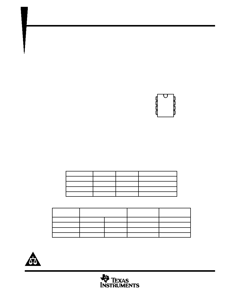
D PACKAGE
(TOP VIEW)
1
2
3
4
8
7
6
5
COMP
VFB
ISENSE
RT/CT
VREF
VCC
OUTPUT
GND
相关PDF资料 |
PDF描述 |
|---|---|
| V62/03633-01XE | SPECIALTY ANALOG CIRCUIT, PDSO16 |
| V62/03665-01YE | 4-CHANNEL, DIFFERENTIAL MULTIPLEXER, PDSO16 |
| V62/03665-01XE | 4-CHANNEL, DIFFERENTIAL MULTIPLEXER, PDSO16 |
| V62/05603-01XE | LOG OR ANTILOG AMPLIFIER, 40 MHz BAND WIDTH, PDSO16 |
| V62/09616-01XE | 4-CHANNEL, SGL ENDED MULTIPLEXER, PDSO14 |
相关代理商/技术参数 |
参数描述 |
|---|---|
| V6203628-01XE | 制造商:TI 制造商全称:Texas Instruments 功能描述:Controlled Baseline One Assembly/Test Site, One Fabrication Site |
| V6203628-02XE | 制造商:TI 制造商全称:Texas Instruments 功能描述:Controlled Baseline One Assembly/Test Site, One Fabrication Site |
| V62-05601-03XA | 制造商:TI 制造商全称:Texas Instruments 功能描述:Digital Signal Processors |
| V62-05601-03ZE | 制造商:TI 制造商全称:Texas Instruments 功能描述:Digital Signal Processors |
| V62-05611-01YE | 制造商:TI 制造商全称:Texas Instruments 功能描述:FAMILY OF 550-A/CH 3- MHZ RAIL-TO-RAIL INPUT/OUTPUT OPERATIONAL AMPLIFIERS |
发布紧急采购,3分钟左右您将得到回复。