- 您现在的位置:买卖IC网 > PDF目录300087 > VCA2615PFBR (TEXAS INSTRUMENTS INC) SPECIALTY ANALOG CIRCUIT, PQFP48 PDF资料下载
参数资料
| 型号: | VCA2615PFBR |
| 厂商: | TEXAS INSTRUMENTS INC |
| 元件分类: | 模拟信号调理 |
| 英文描述: | SPECIALTY ANALOG CIRCUIT, PQFP48 |
| 封装: | GREEN, PLASTIC, TQFP-48 |
| 文件页数: | 11/33页 |
| 文件大小: | 1122K |
| 代理商: | VCA2615PFBR |
第1页第2页第3页第4页第5页第6页第7页第8页第9页第10页当前第11页第12页第13页第14页第15页第16页第17页第18页第19页第20页第21页第22页第23页第24页第25页第26页第27页第28页第29页第30页第31页第32页第33页
VCA2615
SBOS316D JULY 2005 REVISED OCTOBER 2008
www.ti.com
19
In this case, unlike the conventional termination shown in
Figure 60, both the signal voltage and the RS noise are
attenuated by the same factor of two (or 6dB) before being
re-amplified by the A gain setting. This configuration
avoids the extra 3dB degradation because of the
square-root effect described above, which is the key
advantage of the active termination technique. As noted,
the previous explanation ignored the input noise
contribution of the LNP itself. Also, the noise contribution
of the feedback resistor must be included for a completely
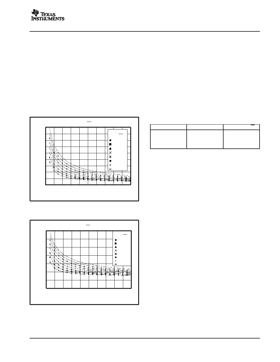
correct analysis. The curves shown in Figure 61 and
Figure 62 allow the VCA2615 user to compare the
achievable noise figure for active and conventional
termination methods.
VCA NOISE = 3.8nV
√Hz, LNP GAIN = 20dB
Source Impedance (
)
0300
100
200
500
400
600
700
800
900 1000
N
o
is
e
F
ig
u
re
(d
B
)
9
8
7
6
5
4
3
2
1
0
6.0E10
8.0E10
1.0E09
1.2E09
1.4E09
1.6E09
1.8E09
2.0E09
LNP Noise
nV/
√Hz
Figure 61. Noise Figure for Active Termination
Source Impedance (
)
0
300
100
200
500
400
600
700
900 1000
800
N
o
is
e
F
ig
u
re
(d
B
)
14
12
10
8
6
4
2
0
VCA NOISE = 3.8nV
√Hz, LNP GAIN = 20dB
LNP Noise
nV/
√Hz
6.0E10
8.0E10
1.0E09
1.2E09
1.4E09
1.6E09
1.8E09
2.0E09
Figure 62. Noise Figure for Conventional
Termination
VOLTAGE-CONTROLLED AMPLIFIER (VCA)—
DETAIL
Figure 63 shows a simplified schematic of the VCA. The
VCA2615 is a true voltage-controlled amplifier, with the
gain expressed in dB directly proportional to a control
signal. This architecture compares to the older VCA
products where a voltage-controlled attenuator was
followed by a fixed-gain amplifier. With a variable-gain
amplifier, the output noise diminishes as the gain reduces.
A variable-gain amplifier, where the output amplifier gain
is fixed, will not show diminished noise in this manner.
Refer to Table 6, which shows a comparison between the
noise performance at different gains for the VCA2615 and
the older VCA2616.
Table 6. Noise vs Gain (RG = 0)
PRODUCT
GAIN (dB)
NOISE RTI (nV/
√Hz)
VCA2615
60
0.7
VCA2615
20
9.0
VCA2616
60
1.1
VCA2616
20
14.0
The VCA accepts a differential input at the +IN and IN
terminals. Amplifier A1, along with transistors Q2 and Q3,
forms a voltage follower that buffers the +IN signal to be
able to drive the voltage-controlled resistor. Amplifier A3,
along with transistors Q27 and Q28, plays the same role
as
A1.
The
differential
signal
applied
to
the
voltage-controlled resistor network is converted to a
current that flows through transistors Q1 through Q4.
Through the mirror action of transistors Q1/Q5 and Q4/Q6,
a copy of this same current flows through Q5 and Q6.
Assuming that the signal current is less than the
programmed clipping current (that is, the current flowing
through transistors Q7 and Q8), the signal current will then
go through the diode bridge (D1 through D4) and be sent
through either R2 or R1, depending upon the state of Q9.
This signal current multiplied by the feedback resistor
associated with amplifier A2, determines the signal
voltage that is designated OUT. Operation of the circuitry
associated with A3 and A4 is identical to the operation of
the previously described function to create the signal
+OUT.
A1 and its circuitry form a voltage-to-current converter,
while A2 and its circuitry form a current-to-voltage
converter. This architecture was adapted because it has
excellent
signal-handling
capability.
A1
has
been
designed to handle a large voltage signal without
overloading, and the various mirroring devices have also
been sized to handle large currents. Good overload
capability is achieved as both the input and output
amplifier are not required to amplify voltage signals.
相关PDF资料 |
PDF描述 |
|---|---|
| VCA2615RGZR | SPECIALTY ANALOG CIRCUIT, PQCC48 |
| VCA3-103-60M00 | CRYSTAL OSCILLATOR, CLOCK, 60 MHz, HCMOS/TTL OUTPUT |
| VCA3-A3F-FREQ | CRYSTAL OSCILLATOR, CLOCK, 0.32768 MHz - 160 MHz, CMOS OUTPUT |
| VCA3-A5D-FREQ | CRYSTAL OSCILLATOR, CLOCK, 0.32768 MHz - 160 MHz, CMOS OUTPUT |
| VCA3-C3H-FREQ | CRYSTAL OSCILLATOR, CLOCK, 0.32768 MHz - 160 MHz, CMOS OUTPUT |
相关代理商/技术参数 |
参数描述 |
|---|---|
| VCA2615PFBT | 功能描述:特殊用途放大器 2Ch Variable Gain Amplifier RoHS:否 制造商:Texas Instruments 通道数量:Single 共模抑制比(最小值): 输入补偿电压: 工作电源电压:3 V to 5.5 V 电源电流:5 mA 最大功率耗散: 最大工作温度:+ 70 C 最小工作温度:- 40 C 安装风格:SMD/SMT 封装 / 箱体:QFN-20 封装:Reel |
| VCA2615RGZR | 功能描述:特殊用途放大器 2-Channel Variable Gain Amplifier RoHS:否 制造商:Texas Instruments 通道数量:Single 共模抑制比(最小值): 输入补偿电压: 工作电源电压:3 V to 5.5 V 电源电流:5 mA 最大功率耗散: 最大工作温度:+ 70 C 最小工作温度:- 40 C 安装风格:SMD/SMT 封装 / 箱体:QFN-20 封装:Reel |
| VCA2615RGZRG4 | 功能描述:特殊用途放大器 2-Channel Variable Gain Amplifier RoHS:否 制造商:Texas Instruments 通道数量:Single 共模抑制比(最小值): 输入补偿电压: 工作电源电压:3 V to 5.5 V 电源电流:5 mA 最大功率耗散: 最大工作温度:+ 70 C 最小工作温度:- 40 C 安装风格:SMD/SMT 封装 / 箱体:QFN-20 封装:Reel |
| VCA2615RGZT | 功能描述:特殊用途放大器 2-Channel Variable Gain Amplifier RoHS:否 制造商:Texas Instruments 通道数量:Single 共模抑制比(最小值): 输入补偿电压: 工作电源电压:3 V to 5.5 V 电源电流:5 mA 最大功率耗散: 最大工作温度:+ 70 C 最小工作温度:- 40 C 安装风格:SMD/SMT 封装 / 箱体:QFN-20 封装:Reel |
| VCA2615RGZTG4 | 功能描述:特殊用途放大器 2-Channel Variable Gain Amplifier RoHS:否 制造商:Texas Instruments 通道数量:Single 共模抑制比(最小值): 输入补偿电压: 工作电源电压:3 V to 5.5 V 电源电流:5 mA 最大功率耗散: 最大工作温度:+ 70 C 最小工作温度:- 40 C 安装风格:SMD/SMT 封装 / 箱体:QFN-20 封装:Reel |
发布紧急采购,3分钟左右您将得到回复。