- 您现在的位置:买卖IC网 > PDF目录1252 > VDRIVE2 (FTDI, Future Technology Devices International Ltd)MOD USB FLASH DRIVE INTERFACE PDF资料下载
参数资料
| 型号: | VDRIVE2 |
| 厂商: | FTDI, Future Technology Devices International Ltd |
| 文件页数: | 4/8页 |
| 文件大小: | 0K |
| 描述: | MOD USB FLASH DRIVE INTERFACE |
| 产品培训模块: | USB Introduction |
| 产品目录绘图: | VDRIVE2 |
| 标准包装: | 5 |
| 系列: | Vinculum |
| 附件类型: | USB 接口模块 |
| 适用于相关产品: | 闪存驱动器 |
| 产品目录页面: | 634 (CN2011-ZH PDF) |
| 其它名称: | 768-1003 |
�� �
�
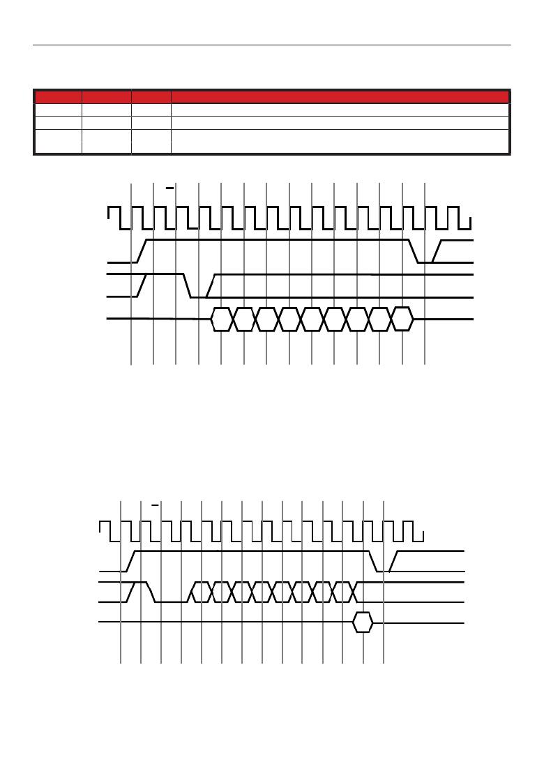
�2.3� SPI� Interface� Signal� Descriptions� and� Timing� Diagrams�
�Ta?le� 3� -� Data� and� Control� ??us� ?ignal� Mode� ?ptions� -� ??I� Inter?ace�
�Page� �
�Pin� No.�
�?�
�4�
�2�
�6�
�Name�
�?CLK�
�?DI�
�?D?�
�C?�
�Type�
�Input�
�Input�
�?utput�
�Input�
�Description�
�??I� Cloc?� input??� 12MHz� ma?imum.�
�??I� ?erial� Data� Input�
�??I� ?erial� Data� ?utput�
�??I� Chip� ?elect� Input�
�Figure� 2� -� ??I� ?lave� Data� ?ead� Cycle�
�R/W� ADD� D7�
�D6�
�D5�
�D4�
�D3�
�D2�
�D1�
�D0�
�SPICLK�
�SPI� CS�
�SPI� Data� In�
�1�
�1�
�0�
�SPI� Data� Out�
�From� ?tart� -� ??I� C?� must� ?e� held� high� ?or� the� entire� read� cycle??� and� must� ?e� ta?en� low� ?or� at� least� one� cloc?� period�
�aft?r� th?� r?ad� i?� co??p??t?d.� Th?� fir?t� bit� on� S??I� Data� In� i?� th?� R/W� bit� -� inp?tting� a� ‘1’� h?r?� a??o??� data� to� b?� r?ad� fro??�
�the� chip.� The� ne?t� ?it� is� the� address� ?it??� ?DD??� which� is� used� to� indicate� whether� the� data� register� (?0?)� or� the� status�
�register� (?1?)� is� read� ?rom.� During� the� ??I� read� cycle� a� ?yte� o?� data� will� start� ?eing� output� on� ??I� Data� ?ut� on� the� ne?t�
�c?ock� cyc??� aft?r� th?� addr???� bit??� MSB� fir?t.� ?ft?r� th?� data� ha?� b??n� c?ock?d� o?t� of� th?� chip??� th?� ?tat??� of� S??I� Data�
�?ut� should� ?e� chec?ed� to� see� i?� the� data� read� is� new� data.� ?� ?0?� level� here� on� ??I� Data� ?ut� means� that� the� data� read�
�is� new� data.� ?� ?1?� indicates� that� the� data� read� is� old� data??� and� the� read� cycle� should� ?e� repeated� to� get� new� data.�
�?emem?er� that� C?� must� ?e� held� low� ?or� at� least� one� cloc?� period� ?e?ore� ?eing� ta?en� high� again� to� continue� with� the�
�ne?t� read� or� write� cycle.�
�Figure� 3� -� ??I� ?lave� Data� Write� Cycle�
�R/W� ADD� D7�
�D6�
�D5�
�D4�
�D3�
�D2�
�D1�
�D0�
�SPICLK�
�SPI� CS�
�SPI� Data� In�
�1�
�0�
�0�
�SPI� Data� Out�
�From� ?tart� -� ??I� C?� must� ?e� held� high� ?or� the� entire� write� cycle??� and� must� ?e� ta?en� low� ?or� at� least� one� cloc?� period�
�aft?r� th?� ?rit?� i?� co??p??t?d.� Th?� fir?t� bit� on� S??I� Data� In� i?� th?� R/W� bit� -� inp?tting� a� ‘0’� h?r?� a??o??� data� to� b?� ?ritt?n�
�to� the� chip.� The� ne?t� ?it� is� the� address� ?it??� ?DD??� which� is� used� to� indicate� whether� the� data� register� (?0?)� or� the� status�
�register� (?1?)� is� written� to.� During� the� ??I� write� cycle� a� ?yte� o?� data� can� ?e� input� to� ??I� Data� In� on� the� ne?t� cloc?� cycle�
�aft?r� th?� addr???� bit??� MSB� fir?t.� ?ft?r� th?� data� ha?� b??n� c?ock?d� in� to� th?� chip??� th?� ?tat??� of� S??I� Data� O?t� ?ho??d� b?�
�VDrive2� Vinculum� VNC1L� Module�
�Datasheet� Version� 0.99�
�?� Future� Technology� Devices� International� Ltd.� 2007�
�相关PDF资料 |
PDF描述 |
|---|---|
| VDSP-SHARC-PCFLOAT | SOFTWARE VISUALDSP++ FOR SHARC |
| VDSP-SHARC-PCFLT-5 | SOFTWARE SHARC PC FLOAT 5 SEAT |
| VF2F2 | MOD VINCULUM USB DRV DUPLICATOR |
| VLP190UF | POLYSWITCH PTC RESET 1.9A STRAP |
| VLP210ULF | POLYSWITCH PTC RESET 2.1A STRAP |
相关代理商/技术参数 |
参数描述 |
|---|---|
| VDRIVE3 | 功能描述:界面模块 USB Host uController Dev Module Vinculum RoHS:否 制造商:4D Systems 产品:Serial Converters 通道/端口数量: 数据速率: 接口类型:USB, UART 工作电源电压:3.3 V, 5 V 最大工作温度: |
| VDRIVE3-LD | 制造商:Future Technology Devices International (FTDI Chip) 功能描述:MOD USB FLASH DRV INTRFACE W/LID |
| VDRS05A014AGE | 制造商:Vishay Angstrohm 功能描述:Var MOV 14VAC/18VDC 100A 22V Radial Ammo Pack |
| VDRS05A014AHE | 制造商:Vishay Angstrohm 功能描述:Var MOV 14VAC/18VDC 100A 22V Radial Ammo Pack |
| VDRS05A014ALE | 制造商:Vishay Semiconductors 功能描述: |
发布紧急采购,3分钟左右您将得到回复。