- 您现在的位置:买卖IC网 > PDF目录18614 > VN2222LLG (ON Semiconductor)MOSFET N-CH 60V 150MA TO-92 PDF资料下载
参数资料
| 型号: | VN2222LLG |
| 厂商: | ON Semiconductor |
| 文件页数: | 1/4页 |
| 文件大小: | 0K |
| 描述: | MOSFET N-CH 60V 150MA TO-92 |
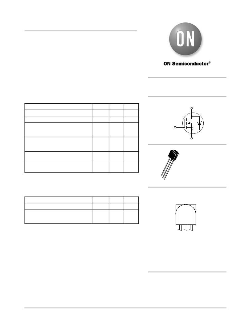
| 产品目录绘图: | MOSFET TO-92 Pkg |
| 标准包装: | 1,000 |
| FET 型: | MOSFET N 通道,金属氧化物 |
| FET 特点: | 逻辑电平门 |
| 漏极至源极电压(Vdss): | 60V |
| 电流 - 连续漏极(Id) @ 25° C: | 150mA |
| 开态Rds(最大)@ Id, Vgs @ 25° C: | 7.5 欧姆 @ 500mA,10V |
| Id 时的 Vgs(th)(最大): | 2.5V @ 1mA |
| 输入电容 (Ciss) @ Vds: | 60pF @ 25V |
| 功率 - 最大: | 400mW |
| 安装类型: | 通孔 |
| 封装/外壳: | TO-226-3、TO-92-3(TO-226AA)成形引线 |
| 供应商设备封装: | TO-92-3 |
| 包装: | 散装 |
| 产品目录页面: | 1558 (CN2011-ZH PDF) |
| 其它名称: | VN2222LLGOS |
�� �
�
�VN2222LLG�
�Small� Signal� MOSFET�
�150� mAmps,� 60� Volts�
�N� ?� Channel� TO� ?� 92�
�Features�
�?� This� is� a� Pb� ?� Free� Device*�
�MAXIMUM� RATINGS�
�http://onsemi.com�
�150� mA,� 60� V�
�R� DS(on)� =� 7.5� W�
�N� ?� Channel�
�Rating�
�Drain� ?� Source� Voltage�
�Drain� ?� Gate� Voltage� (R� GS� =� 1.0� M� W� )�
�Gate� ?� Source� Voltage�
�?� Continuous�
�?� Non� ?� repetitive� (t� p� ≤� 50� m� s)�
�Drain� Current�
�?� Continuous�
�?� Pulsed�
�Symbol�
�V� DSS�
�V� DGR�
�V� GS�
�V� GSM�
�I� D�
�I� DM�
�Value�
�60�
�60�
�±� 20�
�±� 40�
�150�
�1000�
�Unit�
�Vdc�
�Vdc�
�Vdc�
�Vpk�
�mAdc�
�G�
�D�
�S�
�Total� Power� Dissipation� @� T� A� =� 25� °� C�
�Derate� above� 25� °� C�
�Operating� and� Storage� Temperature� Range�
�P� D�
�T� J� ,� T� stg�
�400�
�3.2�
�?� 55� to�
�+150�
�mW�
�mW/� °� C�
�°� C�
�TO� ?� 92�
�CASE� 29�
�STYLE� 22�
�Stresses� exceeding� Maximum� Ratings� may� damage� the� device.� Maximum�
�Ratings� are� stress� ratings� only.� Functional� operation� above� the� Recommended�
�Operating� Conditions� is� not� implied.� Extended� exposure� to� stresses� above� the�
�Recommended� Operating� Conditions� may� affect� device� reliability.�
�THERMAL� CHARACTERISTICS�
�12�
�3�
�MARKING� DIAGRAM�
�Characteristic�
�Thermal� Resistance,� Junction� ?� to� ?� Ambient�
�Maximum� Lead� Temperature� for�
�Soldering� Purposes,� 1/16� ″� from� case�
�for� 10� seconds�
�Symbol�
�R� q� JA�
�T� L�
�Max�
�312.5�
�300�
�Unit�
�°� C/W�
�°� C�
�&� PIN� ASSIGNMENT�
�VN22�
�22LL�
�AYWW� G�
�G�
�1�
�3�
�Source�
�2�
�Drain�
�Gate�
�A� =� Assembly� Location�
�Y� =� Year�
�WW� =� Work� Week�
�G� =� Pb� ?� Free� Package�
�(Note:� Microdot� may� be� in� either� location)�
�ORDERING� INFORMATION�
�See� detailed� ordering� and� shipping� information� in� the� package�
�dimensions� section� on� page� 2� of� this� data� sheet.�
�*For� additional� information� on� our� Pb� ?� Free� strategy� and� soldering� details,� please�
�download� the� ON� Semiconductor� Soldering� and� Mounting� Techniques�
�Reference� Manual,� SOLDERRM/D.�
�?� Semiconductor� Components� Industries,� LLC,� 2011�
�April,� 2011� ?� Rev.� 4�
�1�
�Publication� Order� Number:�
�VN2222LL/D�
�相关PDF资料 |
PDF描述 |
|---|---|
| 199P9S72 | CABLE STR 9POS MALE-FMALE 6' |
| 5512P12P36 | CABLE STR MALE-R/A MALE 12POS 3' |
| 169P144 | CABLE SGL-END STR PLUG 9POS 12' |
| SH513P3S36 | SHLD MINIMIZER STR EXTENSION |
| FDD4685 | MOSFET P-CH 40V 8.4A DPAK |
相关代理商/技术参数 |
参数描述 |
|---|---|
| VN2222LL-G | 功能描述:MOSFET 60V 7.5Ohm RoHS:否 制造商:STMicroelectronics 晶体管极性:N-Channel 汲极/源极击穿电压:650 V 闸/源击穿电压:25 V 漏极连续电流:130 A 电阻汲极/源极 RDS(导通):0.014 Ohms 配置:Single 最大工作温度: 安装风格:Through Hole 封装 / 箱体:Max247 封装:Tube |
| VN2222LL-G P002 | 制造商:Supertex Inc 功能描述:N-CH Enhancmnt Mode MOSFET |
| VN2222LL-G P003 | 制造商:Supertex Inc 功能描述:N-CH Enhancmnt Mode MOSFET |
| VN2222LL-G P005 | 制造商:Supertex Inc 功能描述:N-CH Enhancmnt Mode MOSFET |
| VN2222LL-G P013 | 制造商:Supertex Inc 功能描述:N-CH Enhancmnt Mode MOSFET |
发布紧急采购,3分钟左右您将得到回复。