参数资料
| 型号: | VR1005AAA180-T |
| 厂商: | Taiyo Yuden |
| 文件页数: | 7/9页 |
| 文件大小: | 0K |
| 描述: | VARISTOR 18V 140PF 0402 SMD |
| 标准包装: | 1 |
| 系列: | VR |
| 变阻器电压: | 18V |
| 电流 - 浪涌: | 10A |
| 电路数: | 1 |
| 最大直流电压: | 10VDC |
| 封装/外壳: | 0402(1005 公制) |
| 其它名称: | 587-1418-1 |
�� �
�
�■� PRECAUTIONS�
�Precautions� on� the� use� of� Multilayer� chip� varistors.�
�1.� Circuit� Design�
�◆� Veri?cation� of� operating� environment,� electrical� rating� and� performance�
�1.� A� malfunction� in� medical� equipment,� spacecraft,� nuclear� reactors,� etc.� may� cause� serious� harm� to� human� life� or� have� severe� social� rami?cations.� As� such,�
�any� varistors� to� be� used� in� such� equipment� may� require� higher� safety� and/or� reliability� considerations� and� should� be� clearly� differentiated� from� components�
�Precautions�
�used� in� general� purpose� applications.�
�◆� Operating� Voltage� (Veri?cation� of� Rated� voltage)�
�1.� The� operating� voltage� for� varistors� must� always� be� lower� than� their� rated� values.�
�If� an� AC� voltage� is� loaded� on� a� DC� voltage,� the� sum� of� the� two� peak� voltages� should� be� lower� than� the� rated� value� of� the� varistor� chosen.� For� a� circuit� where�
�both� an� AC� and� a� pulse� voltage� may� be� present,� the� sum� of� their� peak� voltages� should� also� be� lower� than� the� varistor's� rated� voltage.�
�2.� PCB� Design�
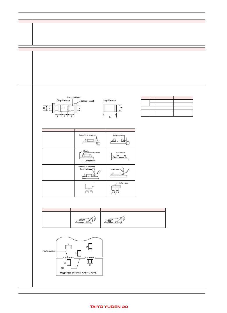
�◆� Pattern� con?gurations� (Design� of� Land-patterns)�
�1.� When� varistors� are� mounted� on� a� PCB,� the� amount� of� solder� used� (size� of� ?llet)� can� directly� affect� varistor� performance.�
�Therefore,� the� following� items� must� be� carefully� considered� in� the� design� of� solder� land� patterns� :�
�(� 1� )� The� amount� of� solder� applied� can� affect� the� ability� of� chips� to� withstand� mechanical� stresses� which� may� lead� to� breaking� or� cracking.� Therefore,� when�
�designing� land-patterns� it� is� necessary� to� consider� the� appropriate� size� and� con?guration� of� the� solder� pads� which� in� turn� determines� the� amount� of�
�Precautions�
�solder� necessary� to� form� the� ?llets.�
�(� 2� )� When� more� than� one� part� is� jointly� soldered� onto� the� same� land� or� pad,� the� pad� must� be� designed� so� that� each� component's� soldering� point� is� separated�
�by� solder-resist.�
�◆� Pattern� con?gurations� (varistor� layout� on� panelized� [breakaway]� PC� boards)�
�1.� After� varistors� have� been� mounted� on� the� boards,� chips� can� be� subjected� to� mechanical� stresses� in� subsequent� manufacturing� processes� (PCB� cutting,�
�board� inspection,� mounting� of� additional� parts,� assembly� into� the� chassis,� wave� soldering� the� re?ow� soldered� boards� etc).� For� this� reason,� planning� pattern�
�con?gurations� and� the� position� of� SMD� varistors� should� be� carefully� performed� to� minimize� stress.�
�◆� Pattern� con?gurations� (Design� of� Land-patterns)�
�1.� The� following� diagrams� and� tables� show� some� examples� of� recommended� patterns� to� prevent� excessive� solder� amounts.� (larger� ?llets� which� extend� above�
�the� component� end� terminations)� Examples� of� improper� pattern� designs� are� also� shown.�
�(� 1� )� Recommended� land� dimensions� for� a� typical� chip� varistor� land� patterns� for� PCBs�
�Recommended� land� dimensions� for� re?ow-soldering�
�Type�
�063�
�1005,� 105C�
�Size�
�A�
�B�
�C�
�L�
�W�
�0.6�
�0.3�
�0.2� ~� 0.30�
�0.2� ~� 0.30�
�0.25� ~� 0.40�
�1.0�
�0.5�
�0.45� ~� 0.55�
�0.40� ~� 0.50�
�0.45� ~� 0.55�
�Unit� :� mm�
�Excess� solder� can� affect� the� ability� of� chips� to� withstand� mechanical� stresses.� Therefore,� please� take� proper� precautions� when� designing� land-patterns.�
�(� 2� )� Examples� of� good� and� bad� solder� application�
�Technical�
�consider-�
�ations�
�Items�
�Mixed� mounting� of� SMD�
�and� leaded� components�
�Component� placement�
�close� to� the� chassis�
�Hand-soldering� of� leaded�
�components� near� mounted�
�components�
�Horizontal� component�
�placement�
�Not� recommended�
�Recommended�
�◆� Pattern� con?gurations� (varistor� layout� on� panelized� [breakaway]� PC� boards)�
�1-1.� The� following� are� examples� of� good� and� bad� varistor� layout;� SMD� varistors� should� be� located� to� minimize� any� possible� mechanical� stresses� from� board� warp�
�or� de?ection.�
�De?ection� of� the� board�
�Not� recommended�
�Recommended�
�Position� the� component�
�at� a� right� angle� to� the� direction�
�of� the� mechanical� stresses� that�
�are� anticipated.�
�1-2.� To� layout� the� varistors� for� the� breakaway� PC� board,� it� should� be� noted� that� the� amount� of� mechanical� stresses� given� will� vary� depending� on� varistor� layout.�
�The� example� below� shows� recommendations� for� better� design.�
�1-3.� When� breaking� PC� boards� along� their� perforations,� the� amount� of� mechanical� stress� on� the� varistors� can� vary� according� to� the� method� used.� The� following�
�methods� are� listed� in� order� from� least� stressful� to� most� stressful:� push-back,� slit,� V-grooving,� and� perforation.� Thus,� any� ideal� SMD� varistor� layout� must� also�
�consider� the� PCB� splitting� procedure.�
�*� This� catalog� contains� the� typical� speci� ?cation� only� due� to� the� limitation� of� space.� When� you� consider� the� purchase� of� our� products,� please� check� our� speci� ?cation.�
�For� details� of� each� product� (characteristics� graph,� reliability� information,� precautions� for� use,� and� so� on),� see� our� Web� site� (http://www.ty-top.com/)� or� CD� catalogs.�
�chipv0102_reli-PRP4�
�12�
�chipv0102_reli_e-01�
�相关PDF资料 |
PDF描述 |
|---|---|
| VR1005AAA120-T | VARISTOR 12V 130PF 0402 SMD |
| PTVS28VP1UP,115 | TVS 600W UNIDIR 28V SOD128 |
| VR1005AAA080-T | VARISTOR 8V 100PF 0402 SMD |
| 950438-6102-AR | CONN SOCKET 38POS 2MM VERT PCB |
| PTVS11VP1UP,115 | TVS 600W UNIDIR 11V SOD128 |
相关代理商/技术参数 |
参数描述 |
|---|---|
| VR1005AAA270-T | 功能描述:压敏电阻 VARISTOR SMD 0402 27V 40pF RoHS:否 制造商:EPCOS 产品:MLV 电压额定值 DC:22 V 电压额定值 AC:17 V 钳位电压:50 V 直径: 峰值浪涌电流:30 A 浪涌能量额定值:75 mJ 电容:74.2 pF 工作温度范围:- 55 C to + 125 C 安装:SMD/SMT 封装:Reel |
| VR1005AAA6R8-T | 制造商:TAIYO YUDEN 功能描述:Cut Tape 制造商:Taiyo Yuden 功能描述:0 |
| VR1005BBA080-T | 功能描述:压敏电阻 VARISTOR SMD 0402 8V 650pF RoHS:否 制造商:EPCOS 产品:MLV 电压额定值 DC:22 V 电压额定值 AC:17 V 钳位电压:50 V 直径: 峰值浪涌电流:30 A 浪涌能量额定值:75 mJ 电容:74.2 pF 工作温度范围:- 55 C to + 125 C 安装:SMD/SMT 封装:Reel |
| VR1005BBA270-T | 功能描述:压敏电阻 VARISTOR SMD 0402 27V 80pF RoHS:否 制造商:EPCOS 产品:MLV 电压额定值 DC:22 V 电压额定值 AC:17 V 钳位电压:50 V 直径: 峰值浪涌电流:30 A 浪涌能量额定值:75 mJ 电容:74.2 pF 工作温度范围:- 55 C to + 125 C 安装:SMD/SMT 封装:Reel |
| VR1005CCA080-T | 制造商:TAIYO YUDEN 功能描述:Cut Tape 制造商:Taiyo Yuden 功能描述:0 |
发布紧急采购,3分钟左右您将得到回复。