- 您现在的位置:买卖IC网 > PDF目录300101 > VRE302KD 1-OUTPUT THREE TERM VOLTAGE REFERENCE, 2.5 V, PDIP8 PDF资料下载
参数资料
| 型号: | VRE302KD |
| 元件分类: | 基准电压源/电流源 |
| 英文描述: | 1-OUTPUT THREE TERM VOLTAGE REFERENCE, 2.5 V, PDIP8 |
| 封装: | DIP-8 |
| 文件页数: | 4/5页 |
| 文件大小: | 434K |
| 代理商: | VRE302KD |
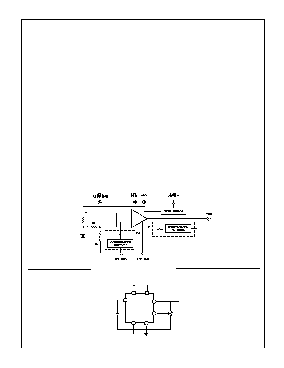
DISCUSSION OF PERFORMANCE
THEORY OF OPERATION
The following discussion refers to the schematic in
figure 2 below. A FET current source is used to bias a
6.3V zener diode. The zener voltage is divided by the
resistor network R1 and R2. This voltage is then applied
to the noninverting input of the operational amplifier which
amplifies the voltage to produce a 2.500V output. The
gain is determined by the resistor networks R3 and R4:
G=1 + R4/R3. The 6.3V zener diode is used because it is
the most stable diode over time and temperature.
The current source provides a closely regulated zener
current, which determines the slope of the references’
voltage vs. temperature function. By trimming the zener
current a lower drift over temperature can be achieved.
But since the voltage vs. temperature function is nonlinear
this compensation technique is not well suited for wide
temperature ranges.
Thaler
Corporation
has
developed
a
nonlinear
compensation network of thermistors and resistors that is
used in the VRE series voltage references. This
proprietary network eliminates most of the nonlinearity in
the voltage vs. temperature function. By adjusting the
slope, Thaler Corporation produces a very stable voltage
over wide temperature ranges.
VRE302
FIGURE 2
VRE302DS REV. F MAY 2001
This network is less than 2% of the overall network
resistance so it has a negligible effect on long term
stability.
Figure 3 shows the proper connection of the VRE302
series voltage references with the optional trim resistor for
initial error.
The VRE302 reference has the ground
terminal brought out on two pins (pin 4 and pin 7) which
are connected together internally. This allows the user to
achieve greater accuracy when using a socket. Voltage
references have a voltage drop across their power supply
ground pin due to quiescent current flowing through the
contact resistance. If the contact resistance was constant
with time and temperature, this voltage drop could be
trimmed out. When the reference is plugged into a socket,
this source of error can be as high as 20ppm. By
connecting pin 4 to the power supply ground and pin 7 to
a high impedance ground point in the measurement
circuit, the error due to the contact resistance can be
eliminated. If the unit is soldered into place, the contact
resistance is sufficiently small that it does not effect
performance. Pay careful attention to the circuit layout to
avoid noise pickup and voltage drops in the lines.
EXTERNAL CONNECTIONS
FIGURE 3
8
4
6
5
+ V
OUT
2
+ V
IN
VRE302
10k
C
N
1F
OPTIONAL
NOISE REDUCTION
CAPACITOR
OPTIONAL
FINE TRIM
ADJUSTMENT
3
V TEMP OUT
7
REF. GND
相关PDF资料 |
PDF描述 |
|---|---|
| VRE302LD | 1-OUTPUT THREE TERM VOLTAGE REFERENCE, 2.5 V, PDIP8 |
| VRE306BD | THREE TERM VOLTAGE REFERENCE, PDIP8 |
| VRE310KS | 1-OUTPUT THREE TERM VOLTAGE REFERENCE, 10 V, PDSO8 |
| VRE402BD | THREE TERM VOLTAGE REFERENCE, PDIP8 |
| VRE402CS | THREE TERM VOLTAGE REFERENCE, PDSO8 |
相关代理商/技术参数 |
参数描述 |
|---|---|
| VRE302KS | 制造商:未知厂家 制造商全称:未知厂家 功能描述:Analog IC |
| VRE302L | 制造商:未知厂家 制造商全称:未知厂家 功能描述:Low Cost Precision Reference |
| VRE302LD | 功能描述:基准电压& 基准电流 Ref. +2.5V, -40/85C 2ppm RoHS:否 制造商:STMicroelectronics 产品:Voltage References 拓扑结构:Shunt References 参考类型:Programmable 输出电压:1.24 V to 18 V 初始准确度:0.25 % 平均温度系数(典型值):100 PPM / C 串联 VREF - 输入电压(最大值): 串联 VREF - 输入电压(最小值): 分流电流(最大值):60 mA 最大工作温度:+ 125 C 封装 / 箱体:SOT-23-3L 封装:Reel |
| VRE302LS | 功能描述:基准电压& 基准电流 Ref. +2.5V, -40/85C 2ppm RoHS:否 制造商:STMicroelectronics 产品:Voltage References 拓扑结构:Shunt References 参考类型:Programmable 输出电压:1.24 V to 18 V 初始准确度:0.25 % 平均温度系数(典型值):100 PPM / C 串联 VREF - 输入电压(最大值): 串联 VREF - 输入电压(最小值): 分流电流(最大值):60 mA 最大工作温度:+ 125 C 封装 / 箱体:SOT-23-3L 封装:Reel |
| VRE303A | 制造商:未知厂家 制造商全称:未知厂家 功能描述:Low Cost Precision Reference |
发布紧急采购,3分钟左右您将得到回复。