- 您现在的位置:买卖IC网 > PDF目录297774 > VRE405KD THREE TERM VOLTAGE REFERENCE, PDIP14 PDF资料下载
参数资料
| 型号: | VRE405KD |
| 元件分类: | 基准电压源/电流源 |
| 英文描述: | THREE TERM VOLTAGE REFERENCE, PDIP14 |
| 封装: | DIP-14 |
| 文件页数: | 4/5页 |
| 文件大小: | 411K |
| 代理商: | VRE405KD |
DISCUSSION OF PERFORMANCE
VRE405DS REV. A MAY 1996
VRE405
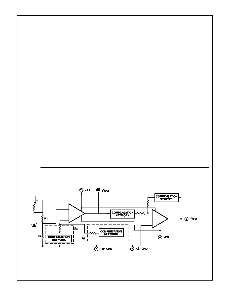
FIGURE 2
THEORY OF OPERATION
The following discussion refers to the schematic in
figure 2 below. A FET current source is used to bias
a 6.3V zener diode. The zener voltage is divided by
the resistor network R1 and R2. This voltage is then
applied to the noninverting input of the operational
amplifier which amplifies the voltage to produce a
5.000V output. The gain is determined by the
resistor networks R3 and R4: G=1 + R4/R3. The
6.3V zener diode is used because it is the most
stable diode over time and temperature.
The current source provides a closely regulated
zener current, which determines the slope of the
references’ voltage vs. temperature function.
By
trimming the zener current a lower drift over
temperature can be achieved. But since the voltage
vs.
temperature
function
is
nonlinear
this
compensation technique is not well suited for wide
temperature ranges.
Thaler Corporation has developed a nonlinear
compensation network of thermistors and resistors
that is used in the VRE series voltage references.
This proprietary network eliminates most of the
nonlinearity in the voltage vs. temperature function.
By adjusting the slope, Thaler Corporation produces
a very stable voltage over wide temperature ranges.
This network is less than 2% of the overall network
resistance so it has a negligible effect on long term
stability.
The VRE405 reference has it’s ground terminal
brought out on two pins (pin 6 and 7) which are
connected internally. This allows the user to achieve
greater accuracy when using a socket. Voltage
references have a voltage drop across their power
supply ground pin due to quiescent current flowing
through the contact resistance. If the contact
resistance was constant with time and temperature,
this voltage drop could be trimmed out. When the
reference is plugged into a socket, this source of
error can be as high as 20ppm. By connecting pin 7
to the power supply ground and pin 6 to a high
impedance ground point in the measurement circuit,
the error due to the contact resistance can be
eliminated. If the unit is soldered into place, the
contact resistance is sufficiently small that it does
not effect performance.
相关PDF资料 |
PDF描述 |
|---|---|
| VRP1-20E1A0G | 1-OUTPUT 100 W DC-DC REG PWR SUPPLY MODULE |
| V7P1-20E1A0 | 1-OUTPUT 100 W DC-DC REG PWR SUPPLY MODULE |
| VRPC-10AT5S | 1-OUTPUT 25 W DC-DC REG PWR SUPPLY MODULE |
| VRPC-10AT5AG | 1-OUTPUT 25 W DC-DC REG PWR SUPPLY MODULE |
| VS-700-LFF-HNN-622.08 | VOLTAGE CONTROLLED CLOCK SAW OSCILLATOR, 622.08 MHz |
相关代理商/技术参数 |
参数描述 |
|---|---|
| VRE405KS | 制造商:未知厂家 制造商全称:未知厂家 功能描述:Analog IC |
| VRE405L | 制造商:未知厂家 制造商全称:未知厂家 功能描述:Precision Dual Reference |
| VRE405LD | 制造商:未知厂家 制造商全称:未知厂家 功能描述:Analog IC |
| VRE405LS | 制造商:未知厂家 制造商全称:未知厂家 功能描述:Analog IC |
| VRE410 | 制造商:未知厂家 制造商全称:未知厂家 功能描述:Precision Dual Reference |
发布紧急采购,3分钟左右您将得到回复。