- 您现在的位置:买卖IC网 > PDF目录361765 > W132-09B Nine Distributed-Output Clock Driver PDF资料下载
参数资料
| 型号: | W132-09B |
| 英文描述: | Nine Distributed-Output Clock Driver |
| 中文描述: | 九分布式输出时钟驱动器 |
| 文件页数: | 5/13页 |
| 文件大小: | 151K |
| 代理商: | W132-09B |
W134M/W134S
Document #: 38-07426 Rev. *A
Page 5 of 13
Table 4
shows the logic for selecting the Bypass and Test
modes. The select bits, S0 and S1, control the selection of
these modes. The Bypass mode brings out the full-speed PLL
output clock, bypassing the Phase Aligner. The Test mode
brings the Refclk input all the way to the output, bypassing
both the PLL and the Phase Aligner. In the Output Test mode
(OE), both the Clk and ClkB outputs are put into a high-imped-
ance state (Hi-Z). This can be used for component testing and
for board-level testing.
Table 5
shows the logic for selecting the Power-down mode,
using the PwrDnB input signal. PwrDnB is active LOW (en-
abled when 0). When PwrDnB is disabled, the DRCG is in its
normal mode. When PwrDnB is enabled, the DRCG is put into
a powered-off state, and the Clk and ClkB outputs are three-
stated.
Table of Frequencies and Gear Ratios
Table 6
shows several supported Pclk and Busclk frequencies,
the corresponding A and B dividers required in the DRCG PLL,
and the corresponding M and N dividers in the gear ratio logic.
The column Ratio gives the Gear Ratio as defined Pclk/Synclk
(same as M and N). The column F@PD gives the divided down
frequency (in MHz) at the Phase Detector, where
F@PD = Pclk/M = Synclk/N.
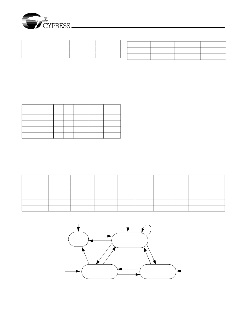
State Transitions
The clock source has three fundamental operating states.
Fig-
ure 4
shows the state diagram with each transition labelled A
through H. Note that the clock source output may NOT be
glitch-free during state transitions.
Upon powering up the device, the device can enter any state,
depending on the settings of the control signals, PwrDnB and
StopB.
In Power-down mode, the clock source is powered down with
the control signal, PwrDnB, equal to 0. The control signals S0
and S1 must be stable before power is applied to the device,
and can only be changed in Power-down mode (PwrDnB = 0).
The reference inputs, V
DDR
and V
DDPD
, may remain on or may
be grounded during the Power-down mode.
Table 3. Clock Stop Mode Selection
Mode
StopB
Normal
Clk Stop
Clk
PAclk
V
X,STOP
ClkB
PAclkB
V
X,STOP
1
0
Table 4. Bypass and Test Mode Selection
Mode
S0
0
0
1
1
S1
0
1
0
1
Bypclk
(int.)
Gnd
-
PLLclk
Refclk
Clk
PAclk
Hi-Z
PLLclk
Refclk
ClkB
PAclkB
Hi-Z
PLLclkB
RefclkB
Normal
Output Test (OE)
Bypass
Test
Table 5. Power-down Mode Selection
Mode
PwrDnB
Normal
Power-down
Clk
PAclk
GND
ClkB
PAclkB
GND
1
0
Table 6. Examples of Frequencies, Dividers, and Gear Ratios
Pclk
Refclk
67
33
100
50
100
50
133
67
133
67
Busclk
267
300
400
267
400
Synclk
67
75
100
67
100
A
8
6
8
4
6
B
1
1
1
1
1
M
2
8
4
4
8
N
2
6
4
2
6
Ratio
1.0
1.33
1.0
2.0
1.33
F@PD
33
12.5
25
33
16.7
Test
M
N
L
K
Normal
Power-Down
Clk Stop
D
C
G
A
E
F
H
V
DD
Turn-On
V
DD
Turn-On
V
DD
Turn-On
V
DD
Turn-On
B
J
Figure 4. Clock Source State Diagram
相关PDF资料 |
PDF描述 |
|---|---|
| W134MH | Miscellaneous Clock Generator |
| W134M | Direct Rambus Clock Generator |
| W134 | Clocks and Buffers |
| W137H | CPU System Clock Generator |
| W13NK100Z | N-channel 1000V - 0.56з - 13A - TO-247 Zener - Protected SuperMESH⑩ PowerMOSFET |
相关代理商/技术参数 |
参数描述 |
|---|---|
| W132-09BX | 制造商:Cypress Semiconductor 功能描述:CLOCK/TIMER:GENERATORS/SYNTHES |
| W132-09BXT | 制造商:Cypress Semiconductor 功能描述:SPREAD AWARE ZERO DELAY BUFFER |
| W132-10B | 制造商:未知厂家 制造商全称:未知厂家 功能描述:Ten Distributed-Output Clock Driver |
| W132-10BX | 制造商:Cypress Semiconductor 功能描述:Zero Delay PLL Clock Buffer Single 25MHz to 140MHz 24-Pin TSSOP 制造商:Rochester Electronics LLC 功能描述:- Bulk |
| W132-10BXT | 制造商:Cypress Semiconductor 功能描述:Zero Delay PLL Clock Buffer Single 25MHz to 140MHz 24-Pin TSSOP T/R 制造商:Rochester Electronics LLC 功能描述:CLK DRIVER - Tape and Reel |
发布紧急采购,3分钟左右您将得到回复。