- 您现在的位置:买卖IC网 > PDF目录361765 > W132-10B Ten Distributed-Output Clock Driver PDF资料下载
参数资料
| 型号: | W132-10B |
| 英文描述: | Ten Distributed-Output Clock Driver |
| 中文描述: | 十分布式输出时钟驱动器 |
| 文件页数: | 2/13页 |
| 文件大小: | 151K |
| 代理商: | W132-10B |
W134M/W134S
Document #: 38-07426 Rev. *A
Page 2 of 13
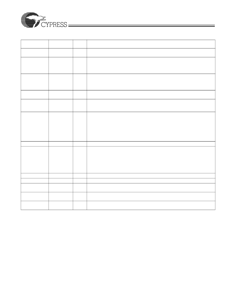
Pin Definitions
Pin Name
REFCLK
Pin
No.
2
Pin
Type
I
Pin Description
Reference Clock Input:
Reference clock input, normally supplied by a system
frequency synthesizer (Cypress W133).
Phase Detector Input:
The phase difference between this signal and SYNCLKN
is used to synchronize the Rambus Channel Clock with the system clock. Both
PCLKM and SYNCLKN are provided by the Gear Ratio Logic in the memory con-
troller. If Gear Ratio Logic is not used, this pin would be connected to Ground.
Phase Detector Input:
The phase difference between this signal and PCLKM is
used to synchronize the Rambus Channel Clock with the system clock. Both
PCLKM and SYNCLKN are provided by the Gear Ratio Logic in the memory con-
troller. If Gear Ratio Logic is not used, this pin would be connected to Ground.
Clock Output Enable:
When this input is driven to active LOW, it disables the
differential Rambus Channel clocks.
Active LOW Power-Down:
When this input is driven to active LOW, it disables the
differential Rambus Channel clocks and places the W134M/W134S in power-down
mode.
PLL Multiplier Select:
These inputs select the PLL prescaler and feedback divid-
ers to determine the multiply ratio for the PLL for the input REFCLK.
PCLKM
6
I
SYNCLKN
7
I
STOPB
11
I
PWRDNB
12
I
MULT 0:1
15, 14
I
CLK, CLKB
S0, S1
20, 18
24, 23
O
I
Complementary Output Clock:
Differential Rambus Channel clock outputs.
Mode Control Input:
These inputs control the operating mode of the
W134M/W134S.
NC
VDDIR
VDDIPD
19
1
10
-
No Connect
Reference for REFCLK:
Voltage reference for input reference clock.
Reference for Phase Detector:
Voltage reference for phase detector inputs and
StopB.
Power Connection:
Power supply for core logic and output buffers. Connected to
3.3V supply.
Ground Connection:
Connect all ground pins to the common system ground
plane.
RefV
RefV
VDD
3, 9, 16, 22
P
GND
4, 5, 8, 13,
17, 21
G
MULT1
0
1
1
0
MULT0
0
0
1
1
W134M
PLL/REFCLK
4.5
6
8
5.333
W134S
PLL/REFCLK
4
6
8
5.333
S1
0
1
0
1
S0
0
0
1
1
MODE
Normal
Output Enable Test
Bypass
Test
相关PDF资料 |
PDF描述 |
|---|---|
| W132-10BX | Ten Distributed-Output Clock Driver |
| W132-09B | Nine Distributed-Output Clock Driver |
| W134MH | Miscellaneous Clock Generator |
| W134M | Direct Rambus Clock Generator |
| W134 | Clocks and Buffers |
相关代理商/技术参数 |
参数描述 |
|---|---|
| W132-10BX | 制造商:Cypress Semiconductor 功能描述:Zero Delay PLL Clock Buffer Single 25MHz to 140MHz 24-Pin TSSOP 制造商:Rochester Electronics LLC 功能描述:- Bulk |
| W132-10BXT | 制造商:Cypress Semiconductor 功能描述:Zero Delay PLL Clock Buffer Single 25MHz to 140MHz 24-Pin TSSOP T/R 制造商:Rochester Electronics LLC 功能描述:CLK DRIVER - Tape and Reel |
| W132E13B | 制造商:OMRON INDUSTRIAL AUTOMATION 功能描述:Discontinued |
| W132MPCX-1 | 制造商:Struthers-Dunn 功能描述: |
| W132MPCX-2 | 制造商:Struthers-Dunn 功能描述: |
发布紧急采购,3分钟左右您将得到回复。