- 您现在的位置:买卖IC网 > PDF目录361766 > W152-11G EIGHT DISTRIBUTED-OUTPUT CLOCK DRIVER|CMOS|SOP|16PIN|PLASTIC PDF资料下载
参数资料
| 型号: | W152-11G |
| 英文描述: | EIGHT DISTRIBUTED-OUTPUT CLOCK DRIVER|CMOS|SOP|16PIN|PLASTIC |
| 中文描述: | 八分布式输出时钟驱动器|的CMOS |专科| 16PIN |塑料 |
| 文件页数: | 4/8页 |
| 文件大小: | 142K |
| 代理商: | W152-11G |
W152
Document #: 38-07148 Rev. **
Page 4 of 8
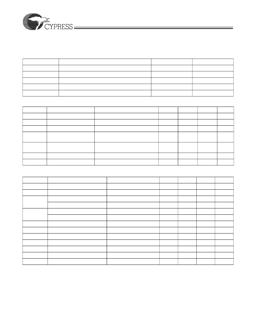
Absolute Maximum Ratings
Stresses greater than those listed in this table may cause per-
manent damage to the device. These represent a stress rating
only. Operation of the device at these or any other conditions
above those specified in the operating sections of this specifi-
cation is not implied. Maximum conditions for extended peri-
ods may affect reliability.
.
Parameter
V
DD
, V
IN
T
STG
T
A
T
B
P
D
Description
Rating
–
0.5 to +7.0
–
65 to +150
0 to +70
–
55 to +125
0.5
Unit
V
°
C
°
C
°
C
W
Voltage on any pin with respect to GND
Storage Temperature
Operating Temperature
Ambient Temperature under Bias
Power Dissipation
DC Electrical Characteristics
:
T
A
=0
°
C to 70
°
C, V
DD
= 3.3V ±10%
Parameter
Description
I
DD
Supply Current
V
IL
Input Low Voltage
V
IH
Input High Voltage
V
OL
Output Low Voltage
Test Condition
Min.
Typ.
Max.
40
0.8
Unit
mA
V
V
V
Unloaded, 100 MHz
2.0
I
OL
= 12 mA (-11, -12)
I
OL
= 8 mA (-1, -2, -3, -4)
I
OH
= 12 mA (-11, -12)
I
OH
= 8 mA (-1, -2, -3, -4)
V
IN
= 0V
V
IN
= V
DD
0.4
V
OH
Output High Voltage
2.4
V
I
IL
I
IH
Input Low Current
Input High Current
50
50
μ
A
μ
A
AC Electrical Characteristics:
T
A
= 0
°
C to +70
°
C, V
DD
= 3.3V ±10%
Parameter
Description
f
IN
Input Frequency
f
OUT
Output Frequency
t
R
Output Rise Time (-1, -2, -3, -4)
Output Rise Time (-11, -12)
t
F
Output Fall Time (-1, -2, -3, -4)
Output Rise Time (-11, -12)
t
ICLKR
t
ICLKF
t
PD
t
SK
Output to Output Skew
t
D
Duty Cycle
t
LOCK
PLL Lock Time
t
JC
Jitter, Cycle-to-Cycle
Notes:
3.
Input frequency is limited by output frequency range and input to output frequency multiplication factor (which is determined by circuit configuration). See
Table 1
.
4.
Longer input rise and fall time will degrade skew and jitter performance.
5.
All AC specifications are measured with a 50
transmission line.
6.
Skew is measured at V
/2 on rising edges.
7.
Duty cycle is measured at V
/2.
8.
For the higher drive -11 and -12, the load is 20 pF.
9.
For frequencies above 25 MHz CY - CY = 125 ps.
10. Measured across all outputs. Maximum skew between outputs in the same bank is 100 ps.
Test Condition
Note 3
15-pF load
[8]
0.8V to 0.8V, 15-pF load
0.8V to 0.8V, 15-pF load
2.0V to 0.8V, 15-pF load
2.0V to 0.8V, 20-pF load
Min.
15
15
Typ.
Max.
140
140
2.5
1.5
2.5
1.5
4.5
4.5
350
215
55
1.0
225
Unit
MHz
MHz
ns
ns
ns
ns
ns
ns
ps
ps
%
ms
ps
2
2
Input Clock Rise Time
[4]
Input Clock Fall Time
[4]
FBIN to REF Skew
[5, 6]
All outputs loaded equally
[10]
15-pF load
[7, 8]
Power supply stable
Note 9
45
50
相关PDF资料 |
PDF描述 |
|---|---|
| W155G | CPU System Clock Generator |
| W156 | Clocks and Buffers |
| W158H | CPU System Clock Generator |
| W159BH | CPU SYSTEM CLOCK GENERATOR|CMOS|SSOP|56PIN|PLASTIC |
| W159H | CPU System Clock Generator |
相关代理商/技术参数 |
参数描述 |
|---|---|
| W152-11X | 制造商:Cypress Semiconductor 功能描述:Zero Delay PLL Clock Buffer Single 15MHz to 140MHz 16-Pin TSSOP 制造商:Rochester Electronics LLC 功能描述:- Bulk |
| W152-11XT | 制造商:Cypress Semiconductor 功能描述:Zero Delay PLL Clock Buffer Single 15MHz to 140MHz 16-Pin TSSOP T/R |
| W152-12G | 功能描述:锁相环 - PLL REMARK TO CY23S08 COM RoHS:否 制造商:Silicon Labs 类型:PLL Clock Multiplier 电路数量:1 最大输入频率:710 MHz 最小输入频率:0.002 MHz 输出频率范围:0.002 MHz to 808 MHz 电源电压-最大:3.63 V 电源电压-最小:1.71 V 最大工作温度:+ 85 C 最小工作温度:- 40 C 封装 / 箱体:QFN-36 封装:Tray |
| W152-12GT | 功能描述:锁相环 - PLL REMARK TO CY23S08 COM RoHS:否 制造商:Silicon Labs 类型:PLL Clock Multiplier 电路数量:1 最大输入频率:710 MHz 最小输入频率:0.002 MHz 输出频率范围:0.002 MHz to 808 MHz 电源电压-最大:3.63 V 电源电压-最小:1.71 V 最大工作温度:+ 85 C 最小工作温度:- 40 C 封装 / 箱体:QFN-36 封装:Tray |
| W152-12X | 制造商:未知厂家 制造商全称:未知厂家 功能描述:Eight Distributed-Output Clock Driver |
发布紧急采购,3分钟左右您将得到回复。