- 您现在的位置:买卖IC网 > PDF目录361765 > W152-2G EIGHT DISTRIBUTED-OUTPUT CLOCK DRIVER|CMOS|SOP|16PIN|PLASTIC PDF资料下载
参数资料
| 型号: | W152-2G |
| 英文描述: | EIGHT DISTRIBUTED-OUTPUT CLOCK DRIVER|CMOS|SOP|16PIN|PLASTIC |
| 中文描述: | 八分布式输出时钟驱动器|的CMOS |专科| 16PIN |塑料 |
| 文件页数: | 3/8页 |
| 文件大小: | 142K |
| 代理商: | W152-2G |
W152
Document #: 38-07148 Rev. **
Page 3 of 8
How to Implement Zero Delay
Typically, zero delay buffers (ZDBs) are used because a de-
signer wants to provide multiple copies of a clock signal in
phase with each other. The whole concept behind ZDBs is that
the signals at the destination chips are all going HIGH at the
same time as the input to the ZDB. In order to achieve this,
layout must compensate for trace length between the ZDB and
the target devices. The method of compensation is described
below.
External feedback is the trait that allows for this compensation.
The PLL on the ZDB will cause the feedback signal to be in
phase with the reference signal. When laying out the board,
match the trace lengths between the output being used for
feedback and the FBIN input to the PLL.
If it is desirable to either add a little delay, or slightly precede
the input signal, this may also be affected by either making the
trace to the FBIN pin a little shorter or a little longer than the
traces to the devices being clocked.
Inserting Other Devices in Feedback Path
Another nice feature available due to the external feedback is
the ability to synchronize signals up to the signal coming from
some other device. This implementation can be applied to any
device (ASIC, multiple output clock buffer/driver, etc.) which is
put into the feedback path.
Referring to
Figure 2
, if the traces between the ASIC/buffer
and the destination of the clock signal(s) (A) are equal in length
to the trace between the buffer and the FBIN pin, the signals
at the destination(s) device will be driven HIGH at the same
time the Reference clock provided to the ZDB goes HIGH.
Synchronizing the other outputs of the ZDB to the outputs form
the ASIC/Buffer is more complex however, as any propagation
delay in the ASIC/Buffer must be accounted for.
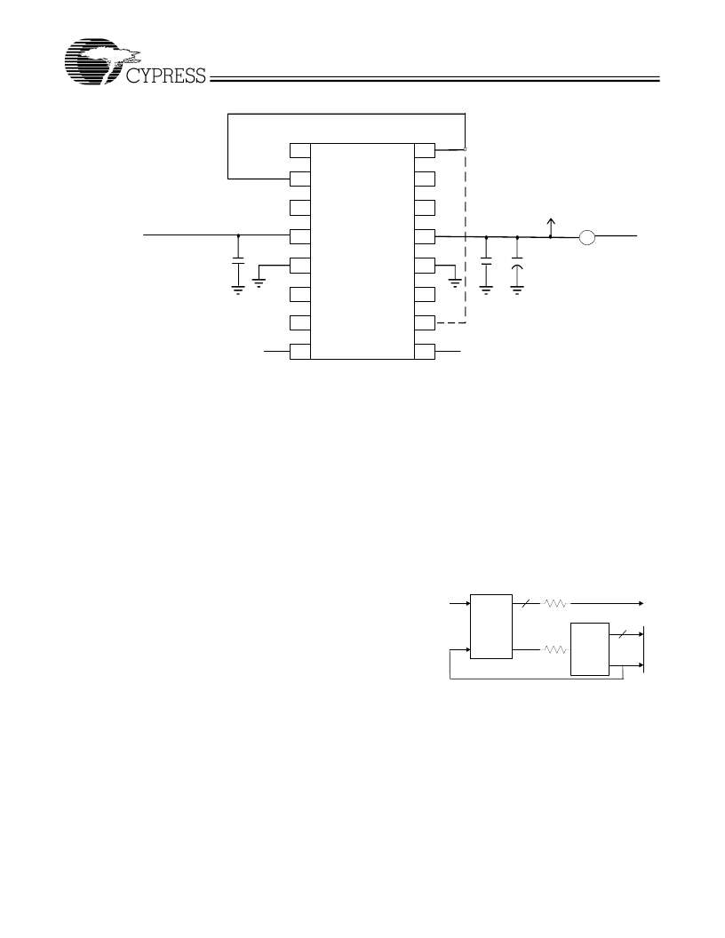
9
2
3
1
4
7
6
8
5
16
13
14
15
10
11
12
3.3V
Supply
VDD
0.1
μ
F
0.1
μ
F10
μ
F
Ferrite
Bead
See Note 3
VDD or GND (for desired operation mo
VDD or GND (for desired operation mode)
QA0
QA2
QA1
QA3
Ground
Power
Power
FB In
Ref In
QB1
QB0
QB2
QB3
SEL1
SEL0
Ground
VDD
Figure 1. Schematic
[3]
Note:
3.
Pin 16 needs to be connected to one of the outputs from either bank A or bank B, it should not be connected to both. Pins 2 and 10 are shown here as
examples. None of the outputs should be considered as preferred for the feedback path.
Reference
Signal
Feedback
Input
ASIC/
Buffer
Zero
Delay
Buffer
A
Figure 2. 6 Output Buffer in the Feedback Path
相关PDF资料 |
PDF描述 |
|---|---|
| W152-2X | Eight Distributed-Output Clock Driver |
| W152-3G | EIGHT DISTRIBUTED-OUTPUT CLOCK DRIVER|CMOS|SOP|16PIN|PLASTIC |
| W152-3X | Eight Distributed-Output Clock Driver |
| W152-4G | EIGHT DISTRIBUTED-OUTPUT CLOCK DRIVER|CMOS|SOP|16PIN|PLASTIC |
| W152-4X | EIGHT DISTRIBUTED-OUTPUT CLOCK DRIVER|CMOS|TSSOP|16PIN|PLASTIC |
相关代理商/技术参数 |
参数描述 |
|---|---|
| W152-2X | 制造商:未知厂家 制造商全称:未知厂家 功能描述:Eight Distributed-Output Clock Driver |
| W152-3G | 制造商:未知厂家 制造商全称:未知厂家 功能描述:EIGHT DISTRIBUTED-OUTPUT CLOCK DRIVER|CMOS|SOP|16PIN|PLASTIC |
| W152-3X | 制造商:未知厂家 制造商全称:未知厂家 功能描述:Eight Distributed-Output Clock Driver |
| W1523X1AEEL WAF | 制造商:ON Semiconductor 功能描述: |
| W152-4G | 制造商:未知厂家 制造商全称:未知厂家 功能描述:EIGHT DISTRIBUTED-OUTPUT CLOCK DRIVER|CMOS|SOP|16PIN|PLASTIC |
发布紧急采购,3分钟左右您将得到回复。